
Ruiqi Precision Measurement: Precision Ceramic Metrology and Inspection Solutions for Semiconductors
From August 26 to 28, 2026, Changzhou Ruiqi Precision Measurement Technology Co., Ltd. will participate in the 8th Aibang Precision Ceramic Industry Chain Exhibition. We invite industry colleagues to visit us at Hall 7, Booth G13, at the Shenzhen World Exhibition & Convention Center for exchanges and discussions.
01
Company Profile
Established in 2017, Changzhou Ruiqi Precision Measurement Technology Co., Ltd. specializes in industrial precision measurement and control solutions, mastering key technologies such as measurement sensors and core algorithms. The company currently operates a 12,000-square-meter facility and employs over 300 staff members, including 90 in R&D and 120 in after-sales service.
Core products include X-ray/beta-ray thickness gauges, line-scan X-ray full-inspection thickness gauges, 3D optical profilometers, and other industrial precision measurement and inspection equipment (such as X-ray imaging systems).
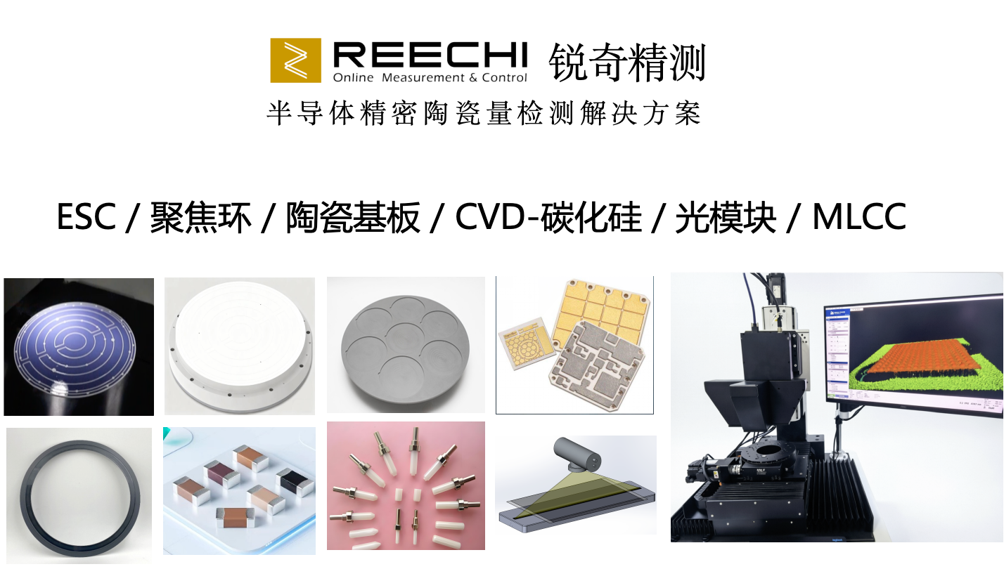
Key market sectors include semiconductor equipment components and precision ceramics, new energy lithium batteries, and various thin films and coatings.
Ruiqi Precision Measurement has an annual production capacity exceeding 2,000 units of its various ray-based and optical thickness gauges and 3D optical profilometers. With annual sales exceeding RMB 400 million, the company ranks among the top three in the domestic market. Its main products hold CE and UL certifications. The company maintains dedicated sales and service teams in the United States, Germany, and South Korea, and exports its products to over 20 countries and regions, including Europe, the Americas, South Korea, and India.
02
Exhibition Introduction
01
Opposed-beam 3D geometric morphology measuring instrument
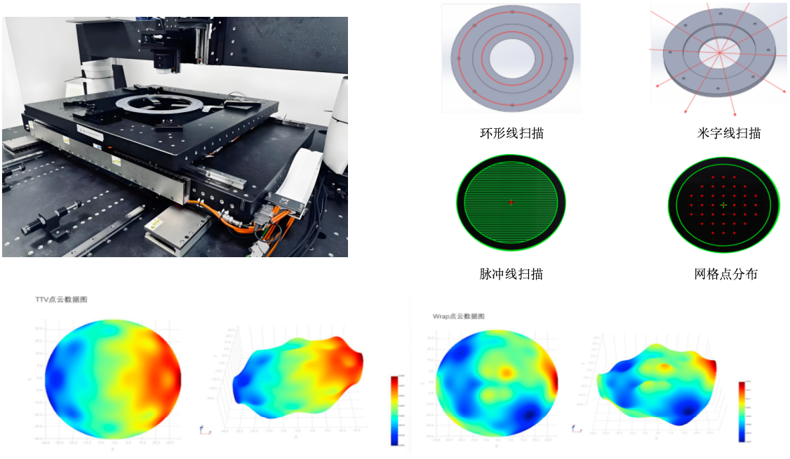
Sensors: Spectral confocal, optical interferometry
Measurement Platform: High-precision multi-axis platform (air-bearing or guideway-based)
Measurement Accuracy: ≤1–5 μm (air-bearing/guideway)
Measurement Parameters: Thickness, TTV, flatness, parallelism, warpage, step height, etc.
Replaces CMMs to achieve efficient measurement, reduce labor, and cut costs while boosting efficiency.
Applications: Geometric profile inspection of substrates, focus rings, electrostatic chucks (ESCs), ceramic substrates, etc.
02
ESC Bump 3D Optical Profiler
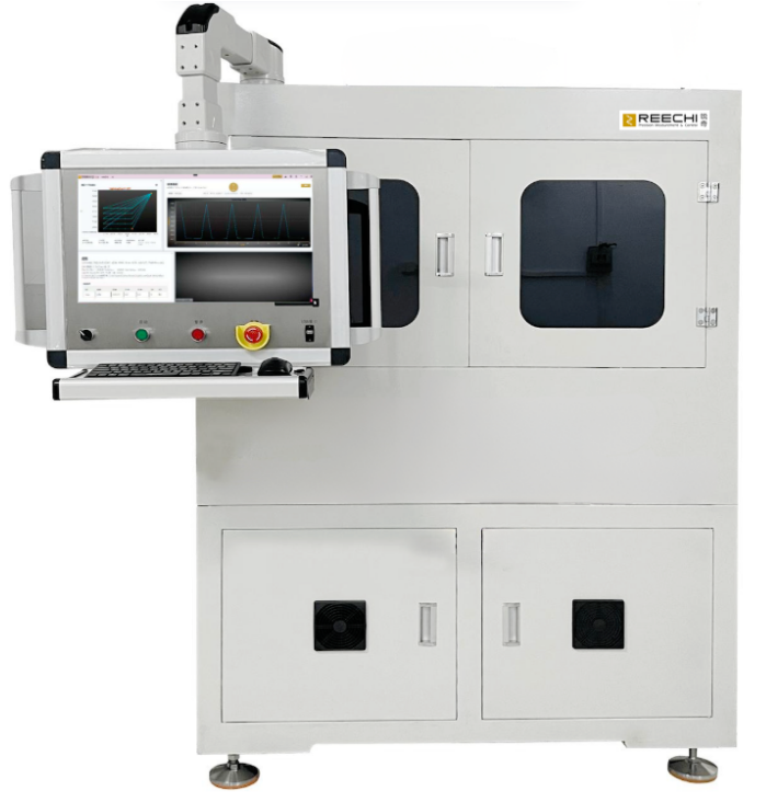
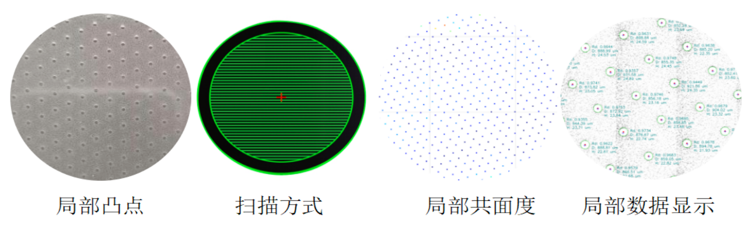
Sensors: Line-scan spectroscopy, white-light interferometry
Measurement Platform: High-precision, multi-axis air-bearing measurement platform
Measurement Accuracy: 0.1–0.5 μm
Applications: Fully automated inspection of electrostatic chucks, covering bump coplanarity, height, diameter, roundness, positional coordinates, surface defects, etc.
Provides comprehensive monitoring and data to support new product R&D and precision refurbishment.
03
Full-inspection X-ray areal density gauge
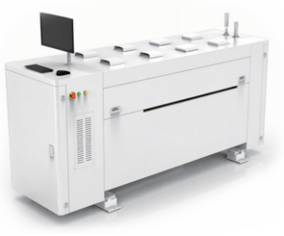
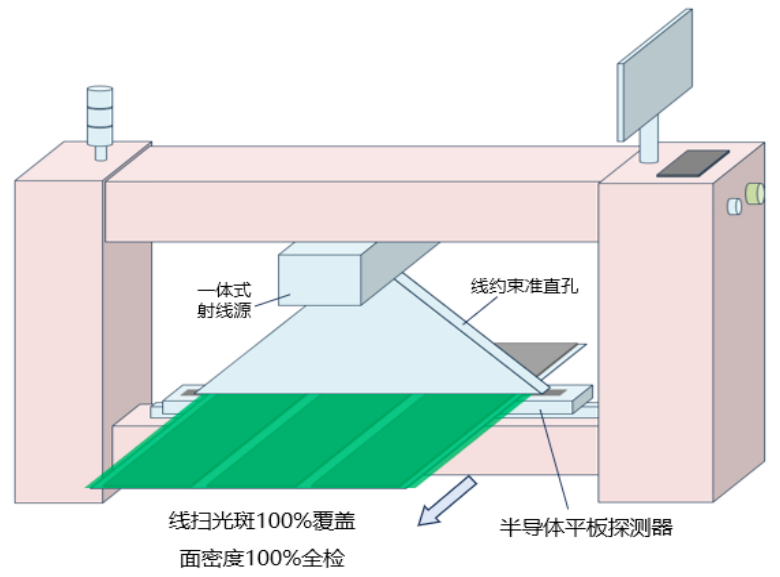
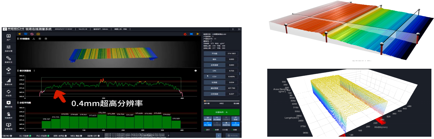
Full-width line-beam X-ray source and full-width linear array flat-panel detector.
Moves beyond traditional "Z-pattern" spot-scanning sampling to achieve 100% full inspection.
Spatial resolution: 0.4 × 0.4 mm pixel size.
Significantly improves areal density uniformity.
100% areal density inspection and 100% data traceability.
Drastically reduces quality control risks.
Provides real-time measurement feedback for efficient closed-loop adjustment.
04
Thickness measurement of printed electrodes on ESCs, ceramic substrates, and MLCCs.
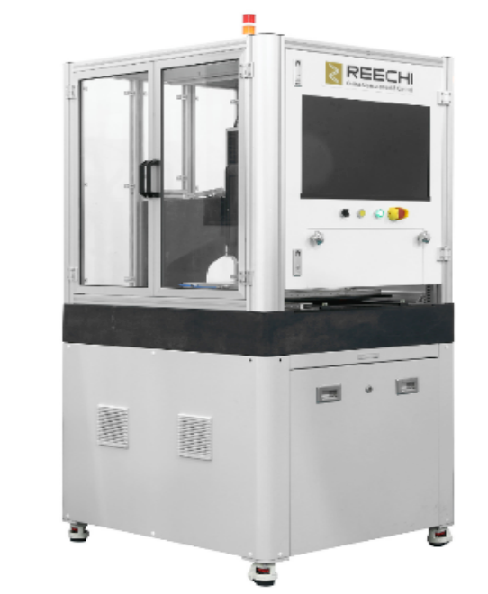
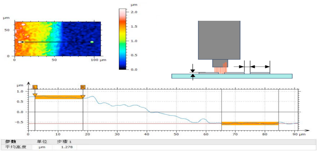
Ultra-high-precision area-scan 3D spectral displacement sensor.
Measurement parameters: thickness and dimensions of printed internal electrode layers, as well as surface topography dimensions.
High-precision granite measurement platform featuring air-bearing or linear motor drive.
Thickness measurement repeatability: 2–10 nm.
Step height differences can be clearly resolved using the RAS100 sensor paired with the R100X objective lens.
05
CVD Silicon Carbide Coating Thickness Gauge
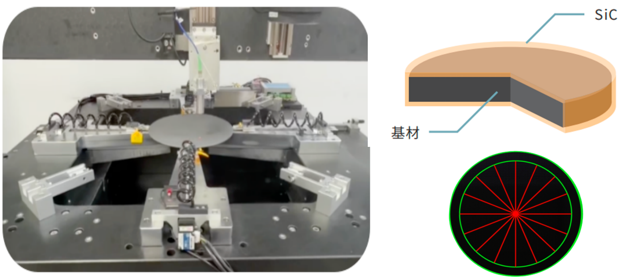
Fully automated measurement of silicon carbide coating thickness on graphite surfaces.
Features automatic calibration and sub-micron precision sensing.
Four-point support design ensures non-destructive testing.
Measurement precision: 10–100 nm (depending on specific material properties).
06
Defect measurement for optical module ceramic ferrules.
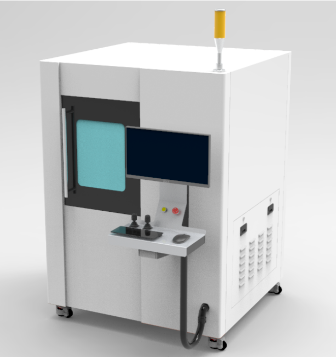
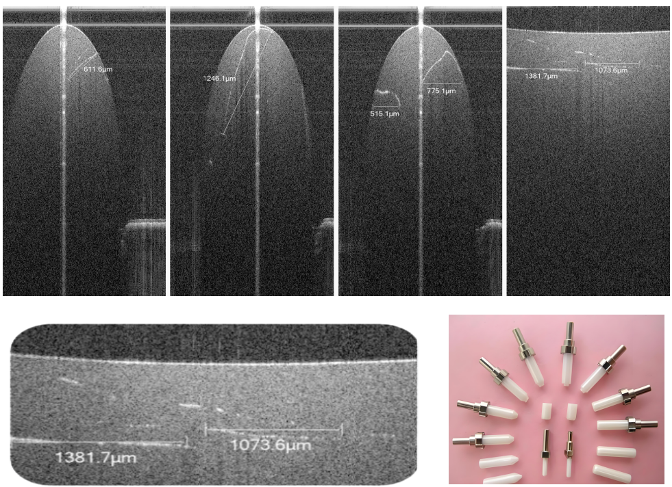
Spectroscopic Tomography Scanner
Non-destructive, transmission-mode inspection for detecting internal, hidden defects.
Synchronous 2D and 3D imaging for comprehensive, all-angle crack detection.
Advanced AI learning capabilities with real-time rejection of defective products.
Recommended Event: [Exhibition Guide] August 26–28 · The 8th Precision Ceramic Industry Chain Exhibition (Shenzhen)
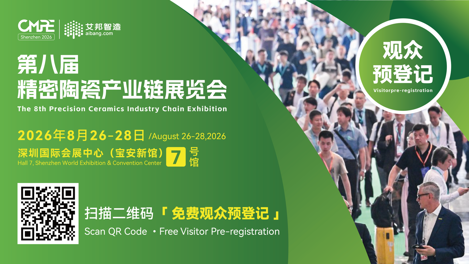
Audience Registration:
1. General Audience Registration
Scan the QR code or copy the link to register:
https://www.aibang360.com/sign/100085
2. VIP Attendee Registration
Benefits for professional VIP attendees: Complimentary drinking water, a lunch voucher, and the exhibition directory.
Benefits for VIP groups (15+ people): Dedicated shuttle service within Guangdong Province.
Target VIP audience sectors: Power semiconductor modules (IGBT/SiC/PIM), packaging & testing, MLCC/LTCC/HTCC, electronic ceramic components, ceramic substrates (AMB/DBC/DPC), communication equipment, optical communication modules, 3C consumer electronics, and automotive electronics.
For VIP and group registration, please contact Ms. Wen at 18126443075 (also her WeChat ID).

※ Admission is restricted to those aged 18 and older; please do not bring children.
Recommended Event #2: One-Click Registration | Free participation in the ten themed forums at the Shenzhen Precision Ceramics Exhibition (August 26–28)!
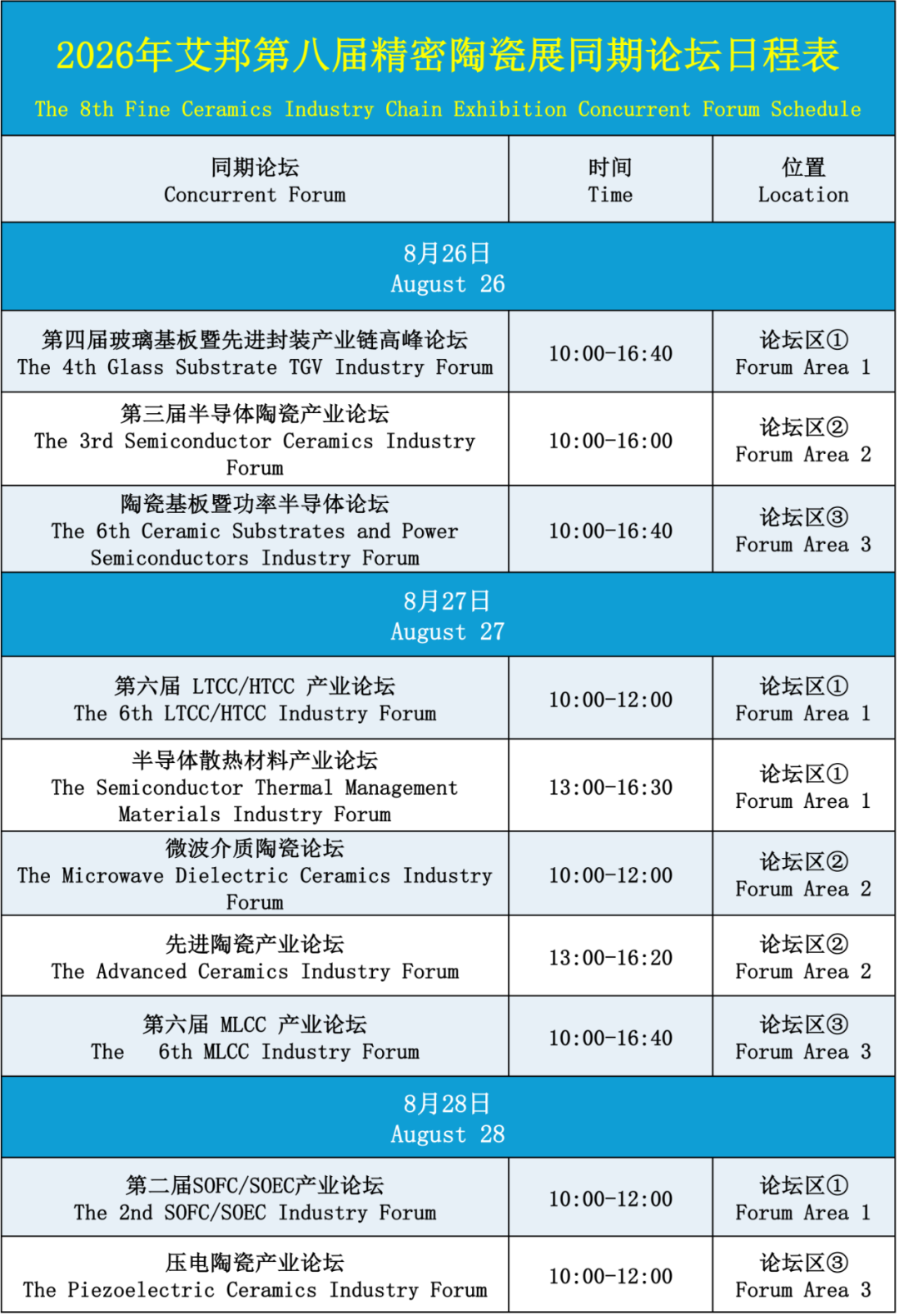
[Free Attendance] How to Register:
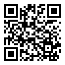
Scan the QR code or copy the link to register.