
Bory Optoelectronics Launches High-Reliability DBA (Direct Bonded Aluminum) Ceramic Substrates for SiC Chip Packaging
From August 26 to 28, 2026, Jiangsu Borui Optoelectronics Co., Ltd. will participate in Aibang’s 8th Precision Ceramic Industry Chain Exhibition (Booth No. G43). We warmly invite industry colleagues to visit us and exchange ideas!
DBA Ceramic Substrates: A Tougher Interface System
As new energy vehicles, photovoltaic energy storage systems, rail transit, and industrial drives evolve toward higher voltages, higher switching frequencies, and higher power densities, the reliability of power modules no longer hinges solely on the substrate's own resistance to thermal cycling. Instead, it depends on whether the integrated interface system—particularly the die-attach interface—can maintain stable performance under repeated thermal shock following the bonding of SiC chips. Addressing this critical factor, Jiangsu BREE Optoelectronics Co., Ltd. (BREE) has recently launched a next-generation DBA (Direct Bonded Aluminum on AlN ceramic) solution for SiC power modules. This solution overcomes the challenge of achieving high-strength bonding between high-purity aluminum and the ceramic insulating layer while leveraging the excellent ductility of aluminum to provide a more resilient interface system for SiC chip packaging (as shown in Figure 1).
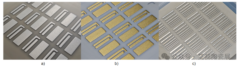
Figure 1: Bory Optoelectronics DBA substrate: (a) Aluminum (Al) pattern on the substrate surface; (b) Al pattern with electroless nickel-gold plating; (c) Demonstration of trace width and spacing gradients.
Bory DBA Ceramic Substrate: Empowering High-Power Devices
The DBA substrate developed by Bory Optoelectronics features an interface free of cold joints, voids, and metallic impurities. It withstands over 5,000 thermal cycling cycles, demonstrating superior thermal cycling performance (as shown in Figure 2).
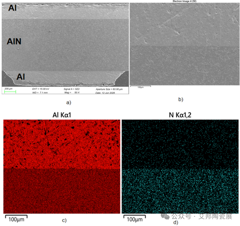
Figure 2. Bory Optoelectronics DBA substrate: (a) interface morphology at 50× magnification; (b) interface morphology at 500× magnification; (c) Al element distribution at the interface; (d) N element distribution at the interface.
Compared to DBC substrates—where Cu/SiC interfaces are prone to the accumulation of thermomechanical stress during thermal cycling, leading to interfacial cracking, delamination, and thermal resistance drift—DBA substrates provide a more stable thermal path and a longer-lasting packaging base for SiC chips. Recent research on SiC/DBA systems, Al interlayers, and Ag-Al interconnections indicates that aluminum-involved interfacial structures help mitigate thermal expansion mismatch, suppress degradation during power cycling, and enhance stability during high-temperature operation. While DBC substrates suffer from chip-substrate delamination after 250 thermal shock cycles, DBA substrates demonstrate significant advantages, showing no significant delamination even after 1,000 cycles.
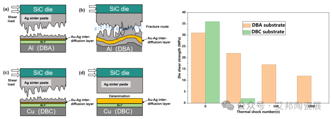
Figure 3: Comparison of chip-bonding interface delamination mechanisms and performance between DBA and DBC substrates.
The DBA substrates launched by Borui Optoelectronics are poised to replace DBC and AMB substrates thanks to their superior thermal conductivity and interface toughness. They are widely compatible with SiC MOSFETs, Schottky Barrier Diodes (SBDs), and high-power half-bridge modules, serving applications such as 800V/1200V traction inverters, PV inverters, energy storage PCS, charging piles, rail transit traction systems, and industrial power supplies. These substrates enable customers to achieve highly reliable packaging designs capable of withstanding more rigorous junction temperature and thermal cycling conditions. The value of DBA substrates lies not only in their excellent resistance to thermal cycling but also in their role as a system-level packaging platform that allows SiC chips to reliably deliver peak performance under real-world operating conditions.
About Borui Optoelectronics
Established in 2009, Jiangsu Borui Optoelectronics Co., Ltd. specializes in rare-earth luminescent materials, high-thermal-conductivity ceramic substrates, and high-thermal-conductivity interface materials. As an industry-leading provider of packaging materials and application solutions for third-generation semiconductors, the company is a domestic pioneer that has fully integrated the entire manufacturing process—spanning powders, sheets (substrates), and metallization—and combines capabilities in original technology, core patents, and the R&D and manufacturing of core products. Borui Optoelectronics’ R&D team has twice been selected for the Jiangsu Provincial "Innovation and Entrepreneurship Team" program; the company boasts a roster of high-level experts, including recipients of national-level talent awards (covering high-level professionals and advanced manufacturing talent), Ministry of Science and Technology innovation and entrepreneurship talent, Jiangsu provincial innovation and entrepreneurship talent, experts from the Jiangsu "333 Project," and honorees of the Jiangsu "Six Major Talent Peaks" initiative.
The company is recognized as a national key "Little Giant" enterprise (specializing in niche markets with cutting-edge technologies), a Jiangsu Province Science and Technology Leading Enterprise, a National High-Tech Enterprise, a Jiangsu Province High-Growth High-Tech Enterprise, and an advanced model unit for standardized intellectual property management. It is a member of the China Rare Earth Industry Association and the National Semiconductor Lighting Engineering R&D and Industry Alliance. The company has established research platforms such as a national postdoctoral research workstation and a Jiangsu provincial enterprise technology center. It has undertaken over 20 national and provincial-level projects—including the National SME Development Special Fund, the Ministry of Science and Technology’s SME Innovation Fund, and Jiangsu provincial programs for the commercialization of scientific achievements and the development of a strong manufacturing province. To date, it holds over 150 granted invention patents (including 44 international patents) and has received two Second Prizes for Jiangsu Science and Technology Progress, one Second Prize for Non-ferrous Metals Industry Science and Technology, and one Second Prize for Technical Standards Excellence from the National Technical Committee on Rare Earths Standardization. Additionally, the company has led or participated in the drafting of 16 national and industry standards.
From August 26 to 28, Borui Optoelectronics will participate in the 8th Aibang Precision Ceramics Exhibition (Booth No. G43). We warmly welcome industry colleagues to visit and exchange ideas!