
Embedded ceramic DPC substrate—a direct upgrade for high-power LED thermal management!
Introduction: As high-power LEDs and power chips become increasingly compact yet more powerful, 70% of the electrical energy is converted into heat that is difficult to dissipate; rapid temperature spikes can lead to issues such as substrate carbonization and total device failure. While traditional FR4 PCBs are inexpensive and easy to process, their poor thermal conductivity makes them unsuitable for high-power applications; conversely, pure ceramic substrates offer excellent heat dissipation but are brittle, costly to process, and involve complex manufacturing techniques. Composite PCB substrates featuring embedded DPC ceramic circuitry combine low cost, ease of routing, and superior heat dissipation, offering the perfect solution to the thermal management challenges of high-power LED packaging.
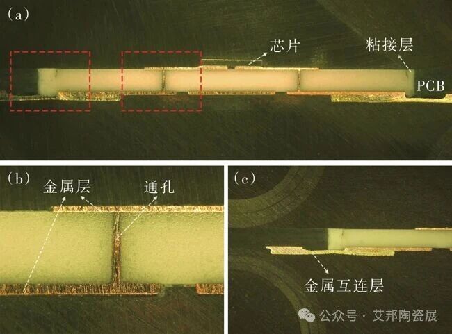
(a) Overall cross-sectional view of the embedded substrate; (b) cross-sectional view of the DPC substrate via; (c) cross-sectional view of the bonding layer of the embedded substrate.
The specific process flow is as follows:
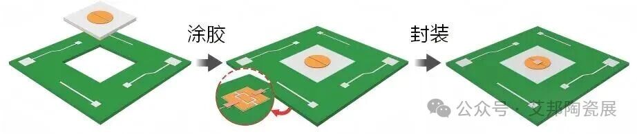
△ Fabrication process for PCB substrates with embedded DPC substrates and their packaging workflow
DPC substrate fabrication: Includes laser drilling, sputter coating (seed layer deposition), dry film lamination, exposure, development, and electroplating for thickening; individual DPC substrates (including circuit layers) are obtained after laser cutting.
PCB substrate: Fabricated via processes such as lamination, dry film lamination, exposure, development, and etching; surface circuitry can undergo Hot Air Solder Leveling (HASL) or Electroless Nickel/Immersion Gold (ENIG) treatment.
Step ①: Create an opening (window) in the PCB substrate; the dimensions of the opening should match those of the DPC substrate.
Step ②: Apply adhesive along the edges of the opening in the PCB substrate and embed the DPC substrate into the opening; cure the adhesive at 150°C for 60 minutes, then grind the edges of the adhesive layer to ensure a flat surface.
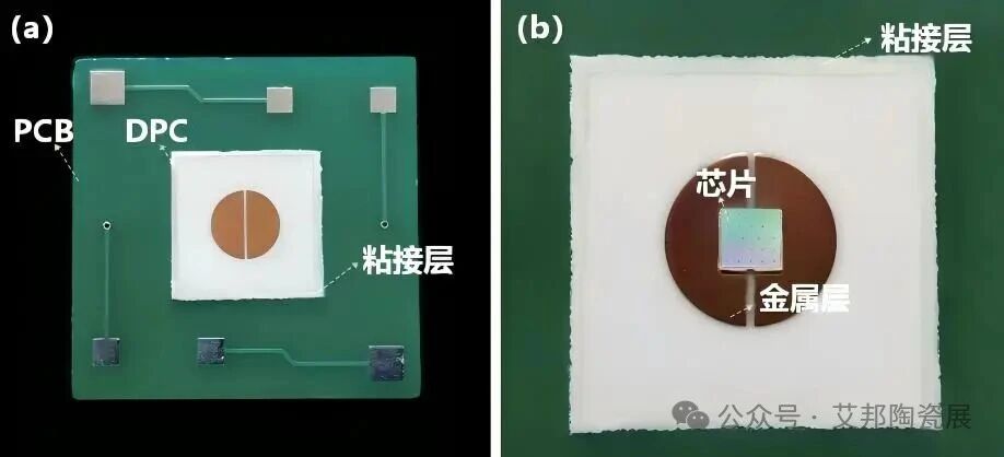
(a) Photograph of the embedded substrate; (b) magnified view of the embedded substrate after LED chip packaging.
Step ③: Deposit a metal layer on the back of the substrate to establish electrical interconnection between the PCB and the DPC substrate, resulting in the complete embedded substrate.
Source: "Preparation of PCB Substrates with Embedded Ceramic Circuit Boards and Their LED Packaging Performance," by Wang Zhe et al.
Aibang has established an industry exchange group for ceramic substrates; you are welcome to join! We invite you to join the WeChat group for the ceramic substrate and packaging industry.
Recommended Event 1: [Concurrent Exhibition Forum] Ceramic Substrate and Power Semiconductor Industry Forum (August 26 · Shenzhen)
(Agenda updated as of July 11)
No. | Proposed Topic | Invited Guest/Speaker |
1 | Innovation in Embedded Packaging Technology Based on DAB Ceramic Substrates | Liu Heng, Head of Strategic Planning Department, Jiangsu Ferrotec Power Semiconductor Research Institute Co., Ltd. |
2 | Silver-Free AMB Copper-Clad Ceramic Substrates for High-Voltage Power Modules: Material Innovation and Reliability Research | Chen Tianhua, Deputy General Manager, Jiangsu Hansirui Semiconductor Technology Co., Ltd. |
3 | Application of Precision Laser Processing and Welding Technologies in High-Reliability Power Device Packaging | Zhao Jiantao, General Manager, Zhejiang Zichen Laser Intelligent Equipment Co., Ltd. |
4 | Silicon Nitride Powder Project via Ammonolysis | Liu Zaixiang, General Manager, Qingdao Qiaohai Ceramic New Materials Technology Co., Ltd. |
5 | Key Technologies and Innovative Applications of DPC Ceramic Substrates for Advanced Packaging | Wu Zhaohui, General Manager, Jiangxi Jinghong New Material Technology Co., Ltd. |
6 | Pioneering Comprehensive Innovative Applications of High-Reliability Silicon Nitride Copper-Clad Ceramic Substrates in New Energy Vehicles, PV Energy Storage, and Industrial Power Modules | Zhou Xin, General Manager, Nantong Wisper Semiconductor Technology Co., Ltd. |
7 | Securing a Position in Domestic Substitution: Mass Production Value and Application Prospects of 92% Alumina Ceramic Substrates | Pan Zimei, Engineer, Guangdong Ciyuan Chuangxin Semiconductor Co., Ltd. |
8 | Application of PVD Technology to Ceramic Substrates for Packaging | Professor Xie Bin, University of Science and Technology of China (USTC) |
9 | Research Progress on IGBT Device Structures | Professor Zhang Jinping, University of Electronic Science and Technology of China (UESTC) |
10 | Applications and Development of High-Performance Aluminum Nitride Ceramics | Wang Mingqing, Deputy Chief Engineer, Chengdu Xuci / Ningxia Beici |
11 | Application of Magnetron Sputtering for Deep-Hole Coating on Ceramic Substrates | Guangdong Huicheng Vacuum Technology Co., Ltd. |
12 | Industrialization and Application of High-Thermal-Conductivity Ceramic Substrates | Peng Xiang, Deputy General Manager/Chief Engineer, Yibin Hongxing Electronics Co., Ltd. |
13 | Topic TBD | Hunan Jinbo Carbon Co., Ltd. |
14 | Discussion on the Application of Silver-Coated Copper in Silver Pastes for Chip Interconnects | Professor Li Minggang, Central South University |
15 | Application of Defect Detection in Precision Ceramic Manufacturing Processes | Liu Weisheng, Deputy General Manager, Shenzhen Hesizhongcheng Technology Co., Ltd. |
We are currently soliciting additional topics; recommendations or self-proposed topics are welcome. For speaking or sponsorship inquiries, please contact Ms. Li at 18124643204 (also her WeChat ID).
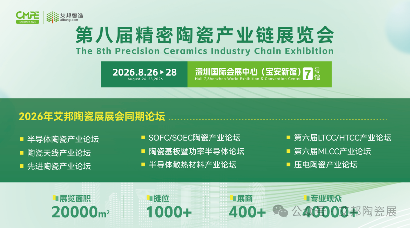
Recommended Event 2: Aibang’s 8th Precision Ceramics Industry Chain Exhibition [August 26–28, 2026 | Hall 7, Shenzhen World Exhibition & Convention Center (Bao'an New Venue)]
Booth Booking:
Ms. Wen: 18126443075 (also WeChat)
Email: wenxiaoting@aibang.com