
Yingxin Semiconductor, a specialized manufacturer of CMP consumables, will participate in the 8th Precision Ceramics Exhibition (August 26–28, Shenzhen).
From August 26 to 28, 2026, Dongguan Yingxin Semiconductor Materials Co., Ltd. will participate in Aibang’s 8th Precision Ceramics Industry Chain Exhibition (Booth No. C43). We warmly invite industry colleagues to visit us and exchange ideas!
Company Profile

Dongguan Yingxin Semiconductor Materials Co., Ltd. was established in June 2021. The company currently operates two major production bases—located in Humen, Dongguan, and Nantong, Jiangsu—with a combined area exceeding 10,000 square meters. These facilities feature cleanroom workshops and are equipped with advanced manufacturing, processing, and testing equipment.
Yingxin is a high-tech enterprise specializing in the R&D, production, and sales of semiconductor CMP (Chemical Mechanical Planarization) consumables. Backed by a professional engineering team, the company designs and optimizes grinding and polishing processes for its customers. Its core products include wax-free vacuum chuck pads, damping cloths, non-woven polishing pads, edge polishing pads, and CMP retaining rings; these products are widely used in the grinding and polishing of materials such as semiconductor crystals, sapphire, ceramics, optics, and metals.
Official Website: http://www.yxbdt.cn/
Product Overview
Corrosion-resistant, wax-free polishing pad
Outer diameter range: 30–572 mm
Pore depth range: 0.15–5.0 mm
Polishing TTV: ≤3 µm
Applications: Polishing of silicon carbide (SiC), gallium nitride (GaN), and similar products
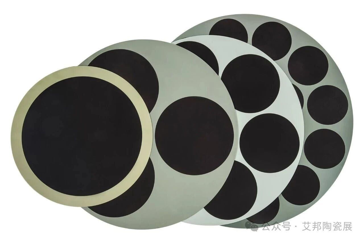
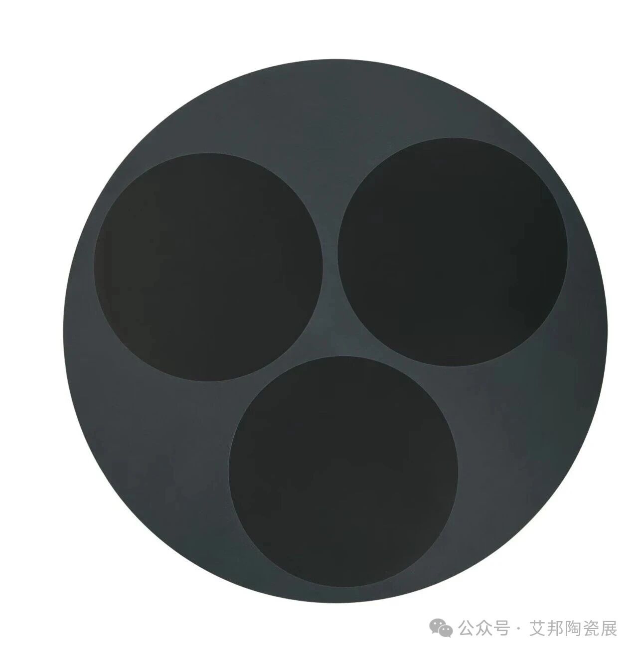
Vacuum-adsorption wax-free pad
Outer diameter range: 30–550 mm
Pore depth range: 0.15–2.0 mm
Polishing TTV performance: ≤5 µm
Used for polishing materials requiring backside immersion, such as gallium arsenide (GaAs), indium phosphide (InP), gallium antimonide (GaSb), and cadmium zinc telluride (CdZnTe).
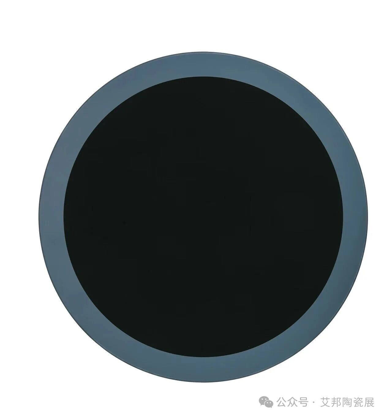
Wax-free polishing pad (velvet type)
Outer diameter range: 30–550 mm
Depth range: 0.15–16 mm
Polishing TTV: ≤3 µm
Used for polishing products such as glass wafers, sapphire, and silicon wafers.
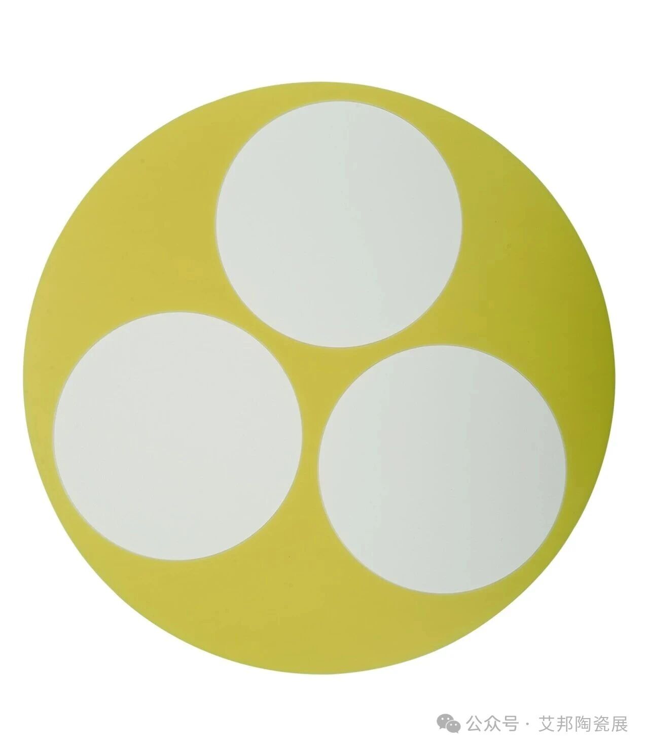
Acid/Alkali-Resistant, Wax-Free Polishing Pad
Outer diameter range: 30–550 mm
Pore depth range: 0.15–2.0 mm
Polishing TTV performance: ≤5 µm
Used for polishing products such as silicon carbide and gallium nitride in strong acid and strong alkali environments.
Damping-cloth polishing pad
This material is elastic and porous, enabling effective pressure transmission, polishing fluid delivery, and debris removal.
During polishing, it effectively retains the polishing fluid, enhancing cutting force while preventing scratches on the workpiece.
It meets requirements for high surface finish and smoothness on the workpiece.
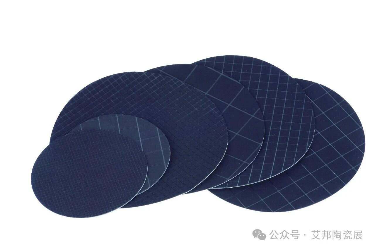
Model | Thickness (mm) | Hardness (Asker C) | Density (g/cm³) |
Damping Cloth Polishing Pad | 0.45–1.8 | 43–89 | 0.3–0.45 |
Available in a full range of specifications; processing options such as adhesive backing, embossing, and grooving are available upon customer request. | |||
Non-woven polishing pad
This material offers high wear resistance, minimal fiber shedding, and a long service life.
It retains polishing fluid well while maintaining moderate rigidity.
It delivers a high polishing rate and excellent surface finish.
It is convenient to use; it can be attached directly to the polishing platen and is easy to mount and remove.
The backing features a highly water-resistant adhesive film that is easy to peel off without leaving residue.
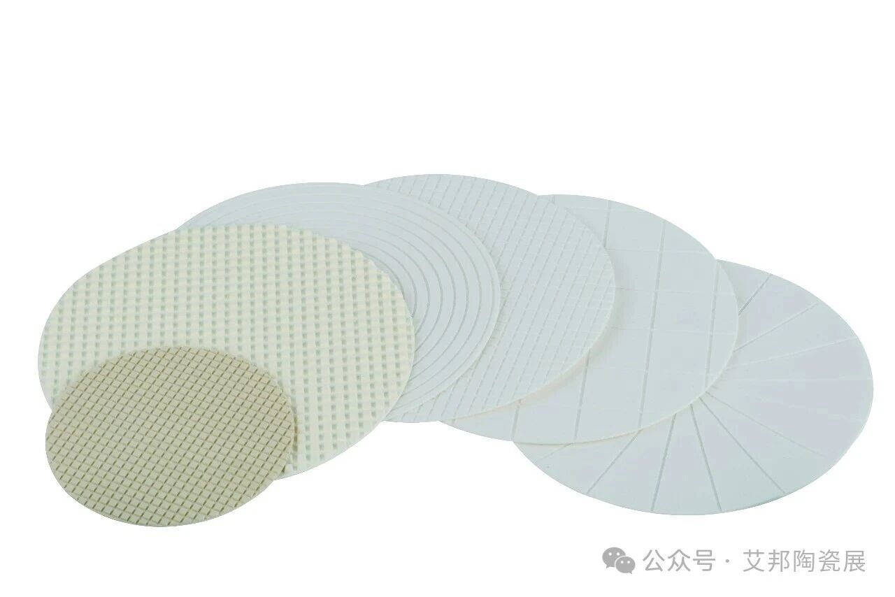
Model | Thickness (mm) | Hardness (Asker C) | Density (g/cm³) |
Non-woven polishing pad | 1–4 | 65–93 | 0.35–0.55 |
Available in a full range of sizes; adhesive backing and grooving can be customized according to customer requirements. Grooving patterns include grid, pyramid, radial, concentric circle, etc. | |||
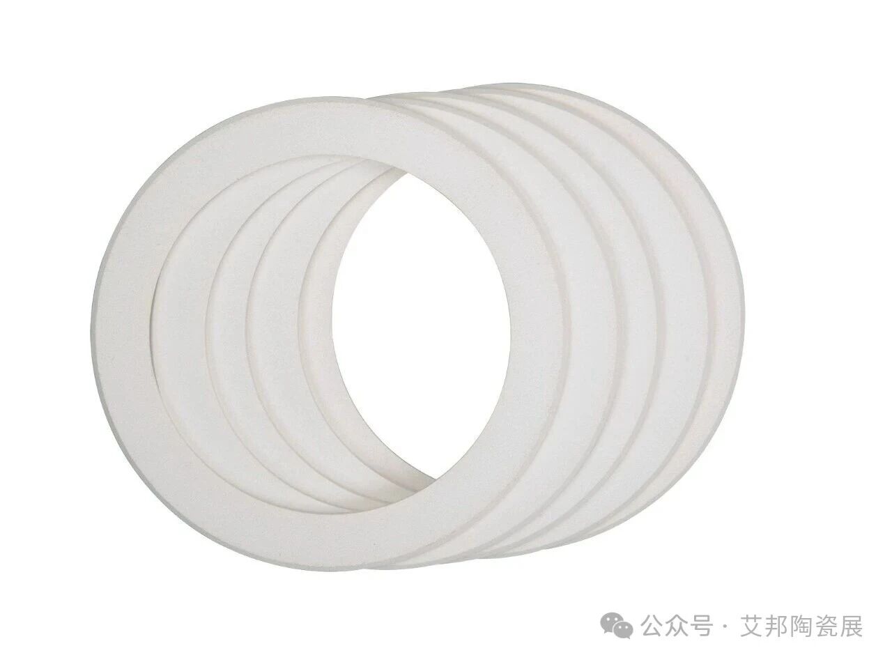
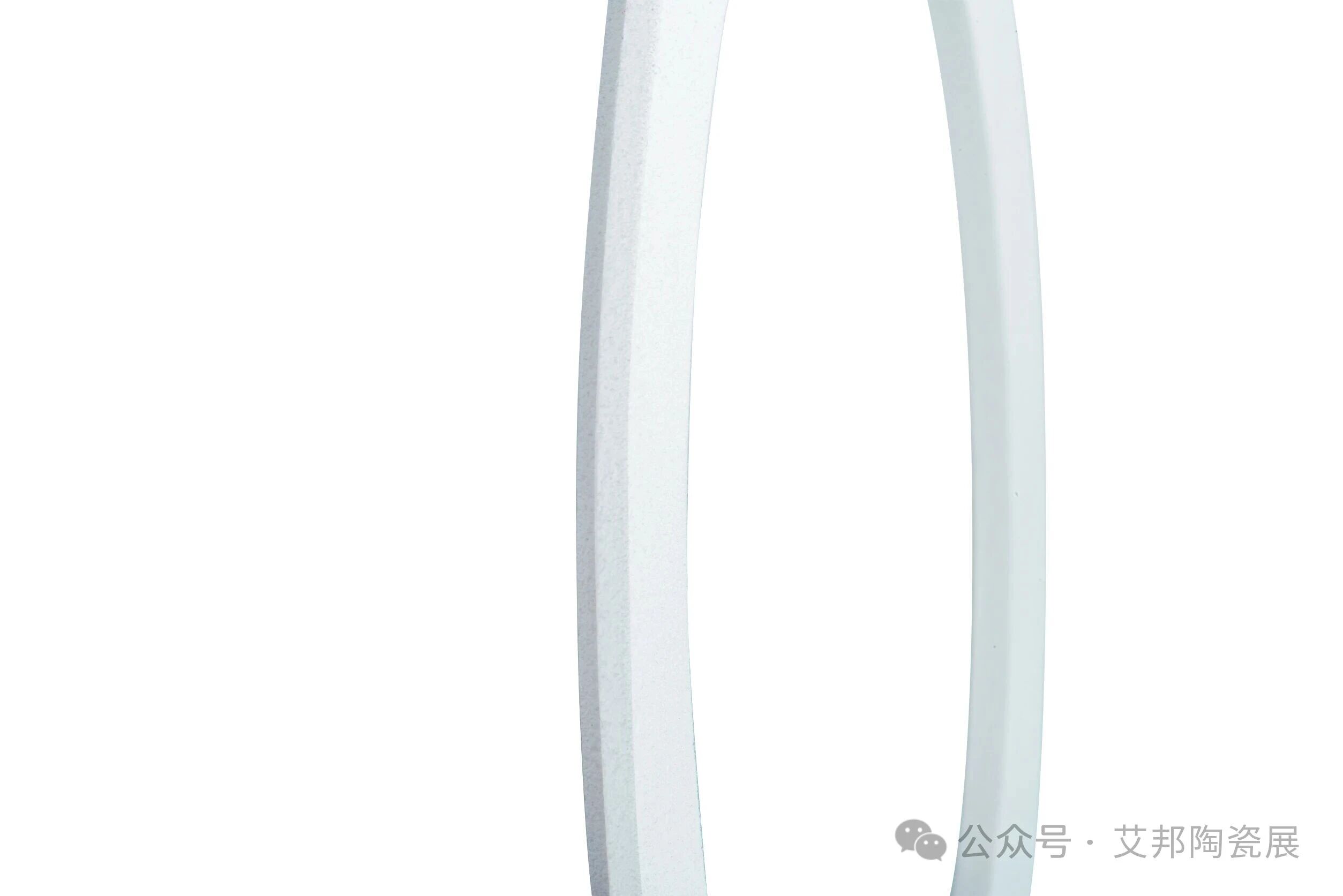
Notch Pad
The Notch ring is a specialized product used on automatic edge-beveling machines (such as those from BBS Jinming). Few domestic suppliers offer this type of Notch Pad; however, Yingxin’s products match the quality standards of Japanese and Korean manufacturers while offering superior cost-effectiveness.
Chuck Pad
Used on wafer chucks
Provides cushioning and wafer protection
Customizable according to customer requirements
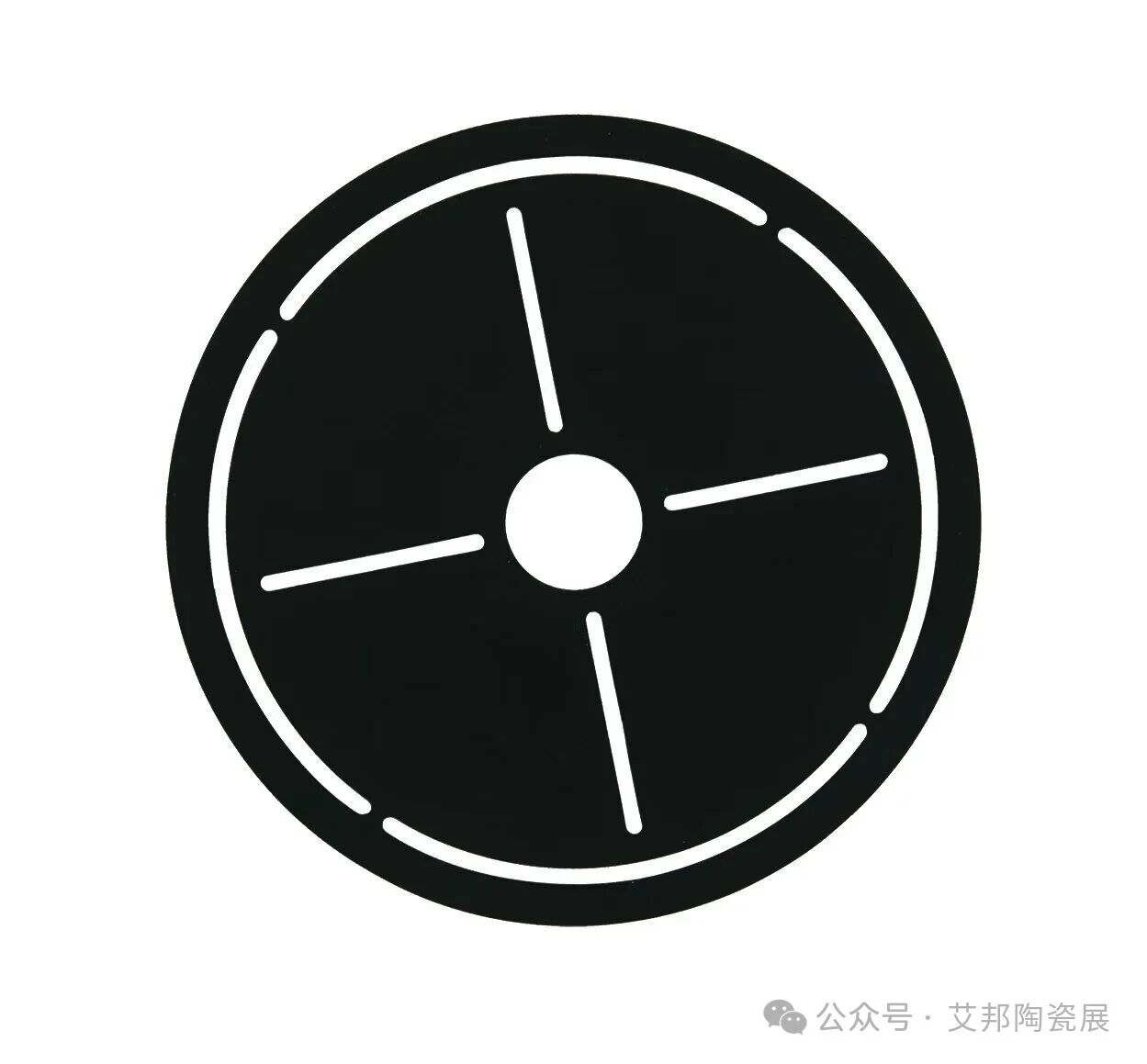
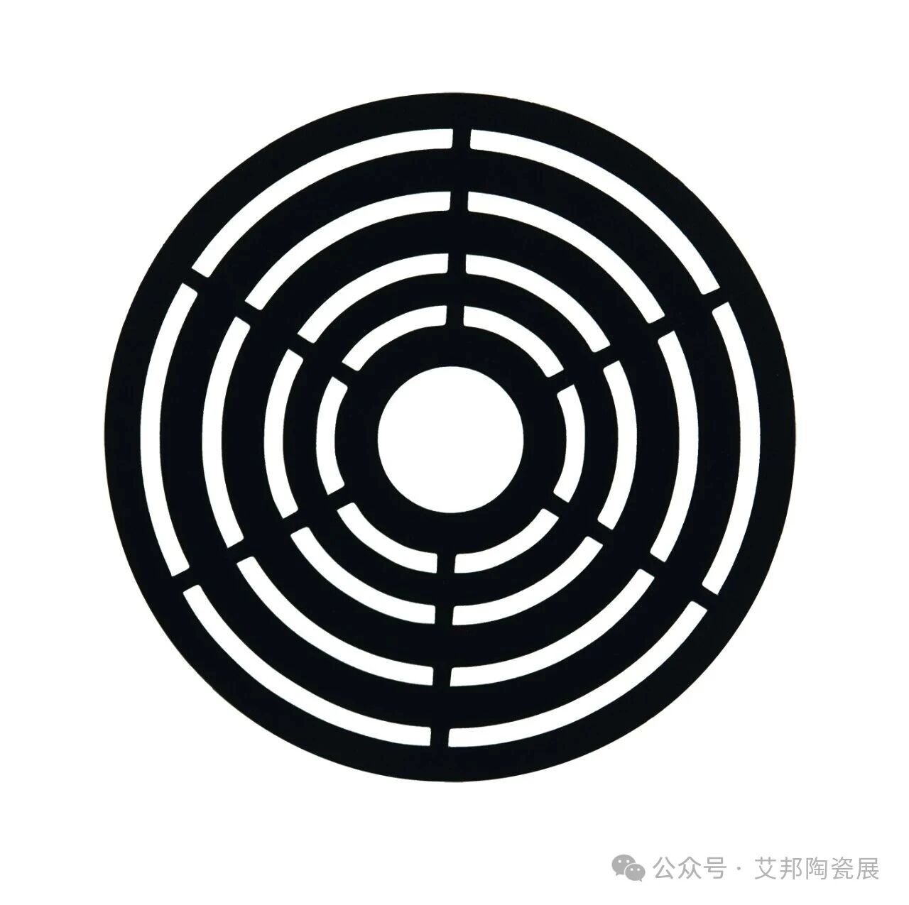
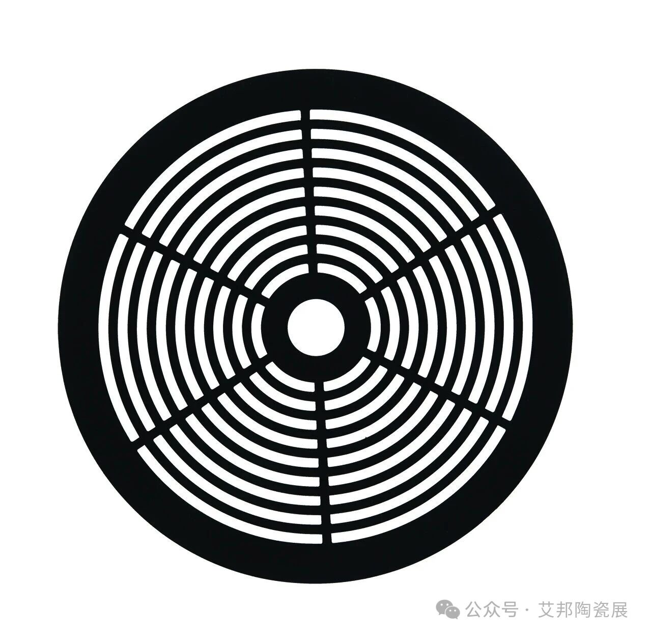
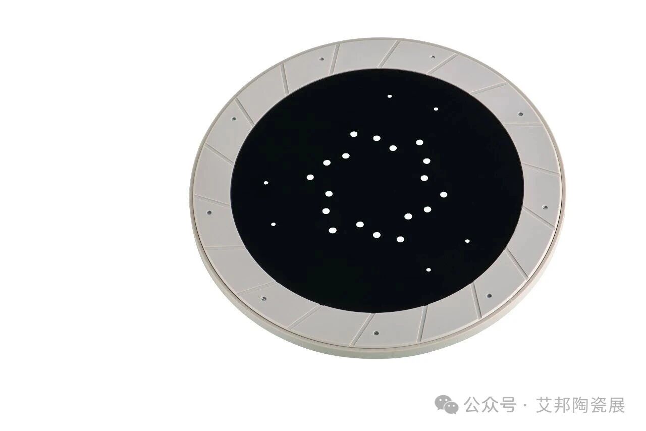
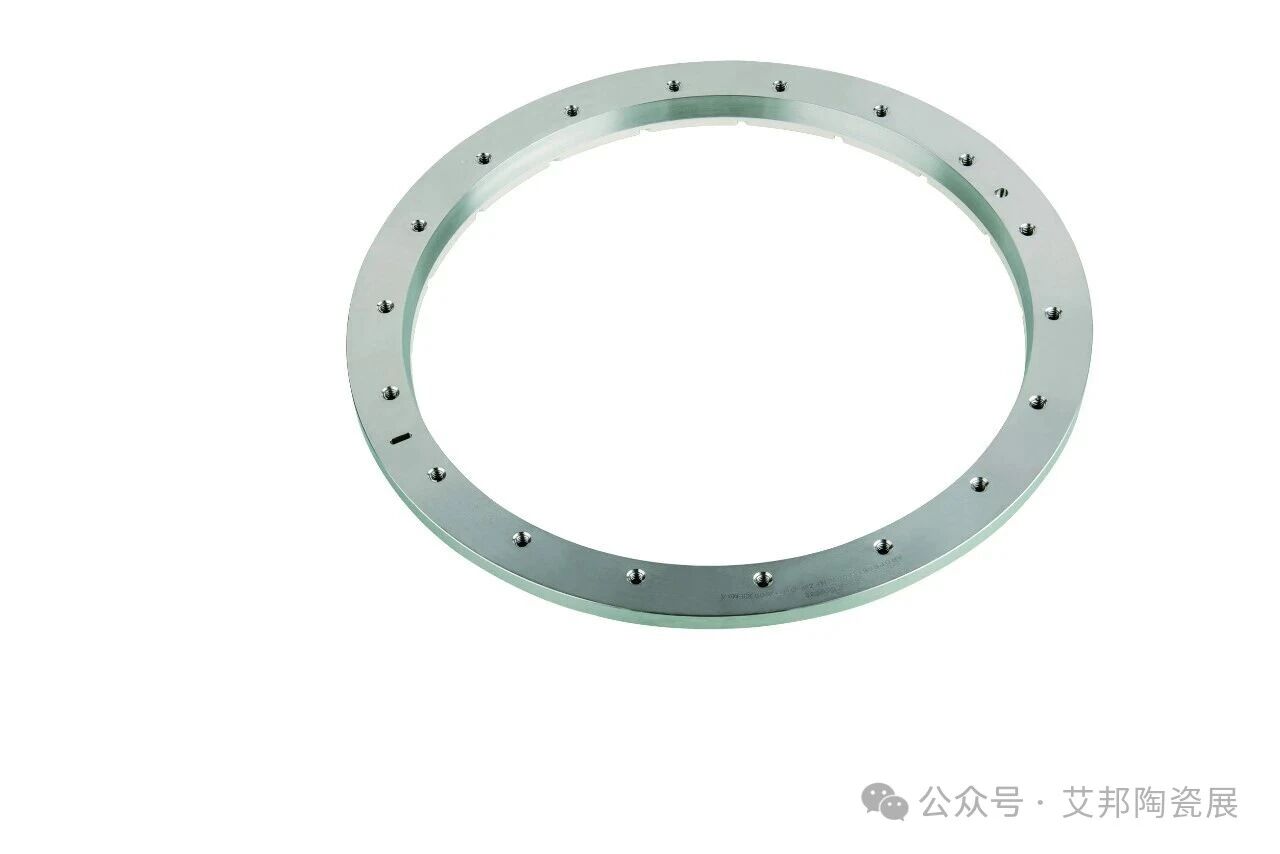
Retaining ring
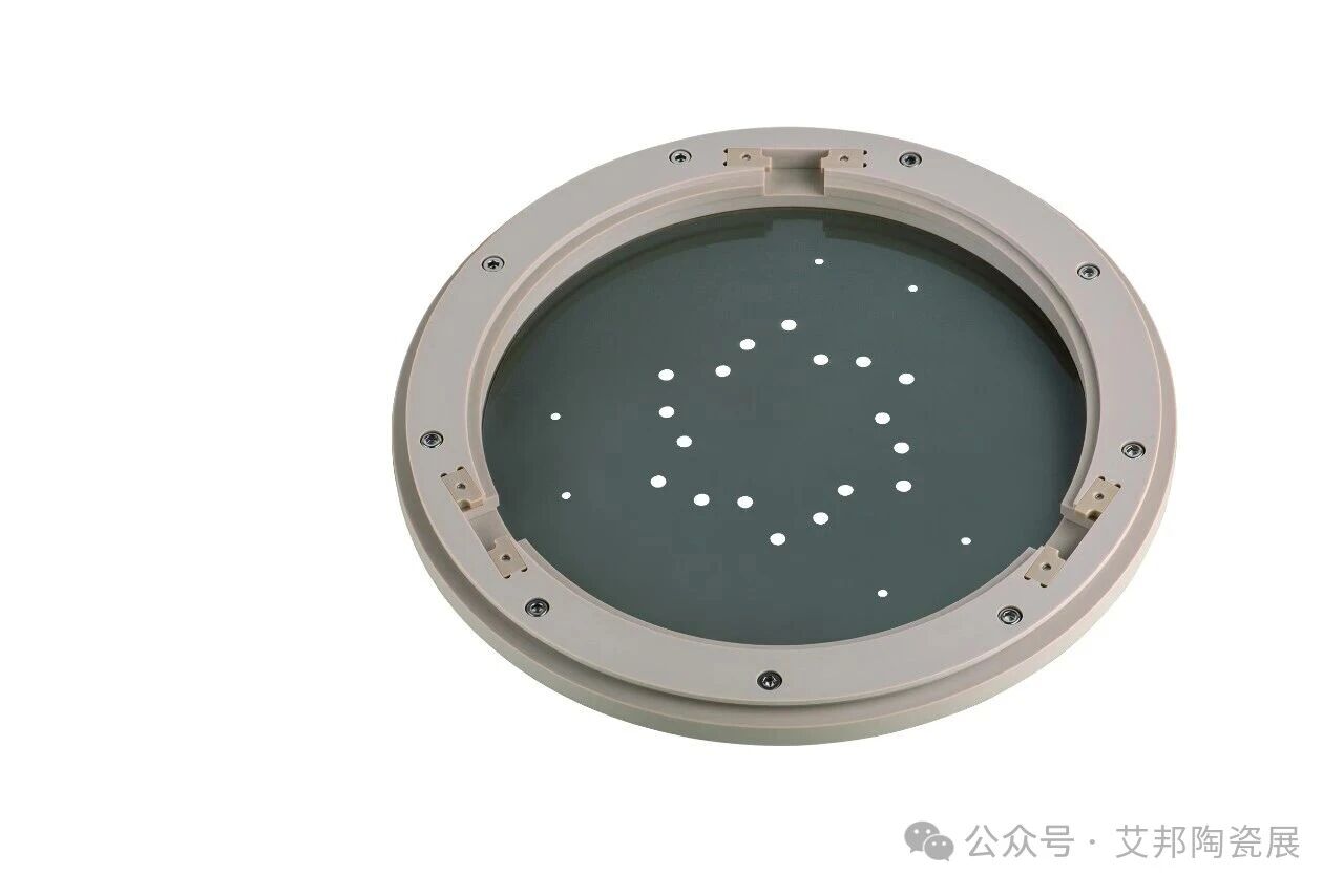
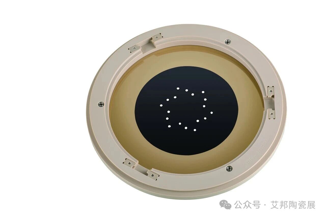
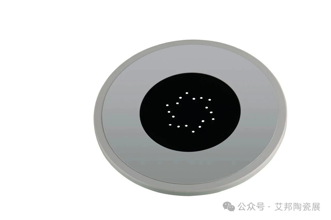
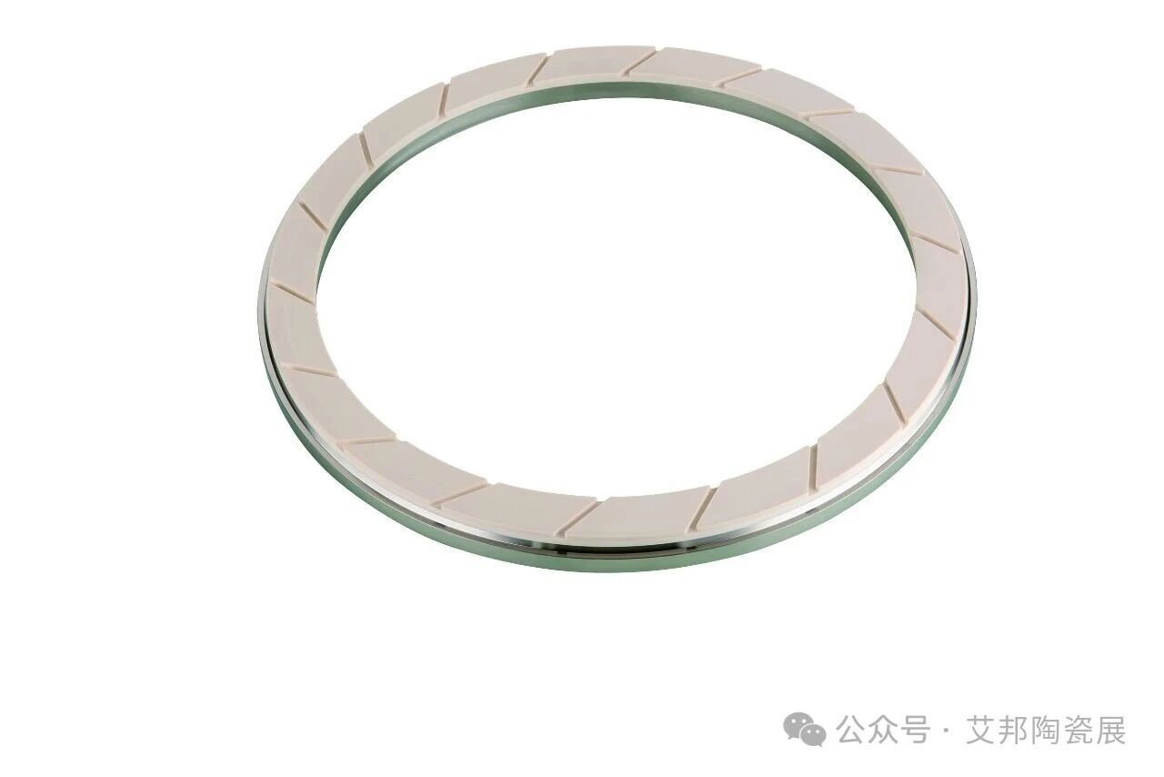
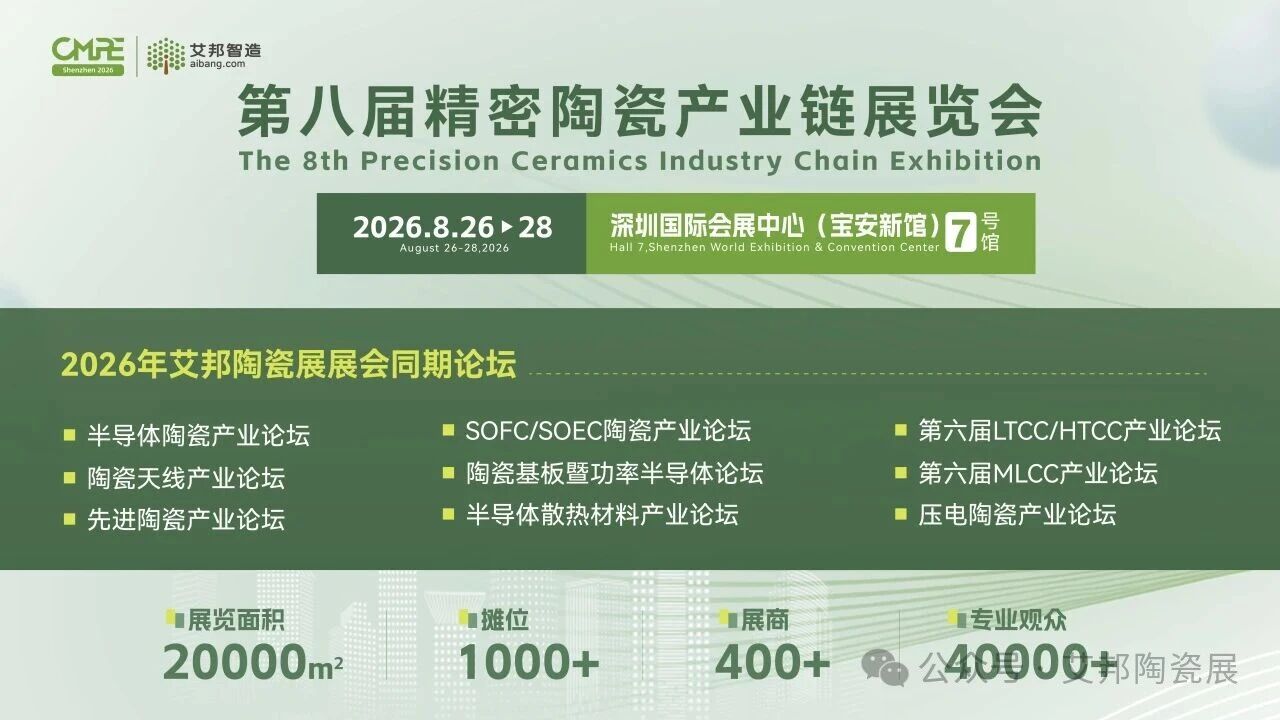
Recommended Event 1: Aibang’s 8th Precision Ceramics Industry Chain Exhibition [August 26–28, 2026 | Hall 7, Shenzhen World Exhibition & Convention Center (Bao'an New Venue)]
Booth Booking
Ms. Li: 18823755657 (WeChat ID)
Ms. Wen: 18126443075 (WeChat ID)
Email: lirongrong@aibang.com
Scan the QR code to add us on WeChat and inquire about exhibition details.

Recommended Event 2: 9 Concurrent Forums
Concurrent Forums at the 8th Precision Ceramics Industry Chain Exhibition | |
6th LTCC/HTCC Industry Forum | 6th MLCC Industry Forum |
Semiconductor Thermal Management Materials Industry Forum | SOFC/SOEC Ceramics Industry Forum |
Ceramic Substrate and Power Semiconductor Industry Forum | Advanced Ceramics Industry Forum |
Piezoelectric Ceramics Industry Forum | Semiconductor Ceramics Industry Forum |
Microwave Dielectric Ceramics Industry Forum | |
How to register as an attendee:

Scan the QR code or copy the link to register.