
How can the microstructure of ceramic materials be precisely characterized? Thermo Fisher’s one-stop microscopy analysis solution.
Thermo Fisher Scientific
From August 26 to 28, 2026, Thermo Fisher Scientific will participate in Aibang’s 8th Precision Ceramics Industry Chain Exhibition (Booth No. C03). We warmly welcome industry colleagues to visit us and exchange ideas!
01
Company Profile
Thermo Fisher’s innovative electron microscopy, surface analysis, and microanalysis solutions empower materials science researchers to advance sample characterization, enabling a deeper understanding of material properties—both physical and chemical—across scales ranging from the macro to the nanoscale.
Thermo Fisher’s multi-scale, multi-modal solutions support a wide range of applications across dozens of industries and research fields, serving a diverse customer base in academia, government, and industry. By combining high-resolution imaging with multi-scale, multi-modal analysis—covering physical, chemical, elemental, mechanical, and electrical properties—the company’s portfolio (including transmission electron microscopes, DualBeam™ focused ion beam/scanning electron microscopes, a full range of SEMs, X-ray photoelectron spectrometers (XPS), microanalysis solutions, and software suites) transforms customer inquiries into actionable data.
02
Product Introduction
The latest generation of aberration-corrected transmission electron microscopes—
Iliad (Scanning) Transmission Electron Microscope
Iliad™ is a fully integrated analytical (scanning) transmission electron microscope equipped with the all-new Iliad™ electron energy loss spectrometer (EELS) and energy filter, a dedicated Zebra EELS detector, and the brand-new NanoPulser ultrafast electrostatic beam blanker; it also supports integration with Dual-X, Super-X™, or Ultra-X EDX detectors. With unprecedented hardware and software integration and a forward-looking approach to instrument design, the Iliad™ (S)TEM opens a new chapter in aberration-corrected electron microscopy.
Helios 5 Ga+ DualBeam Microscope
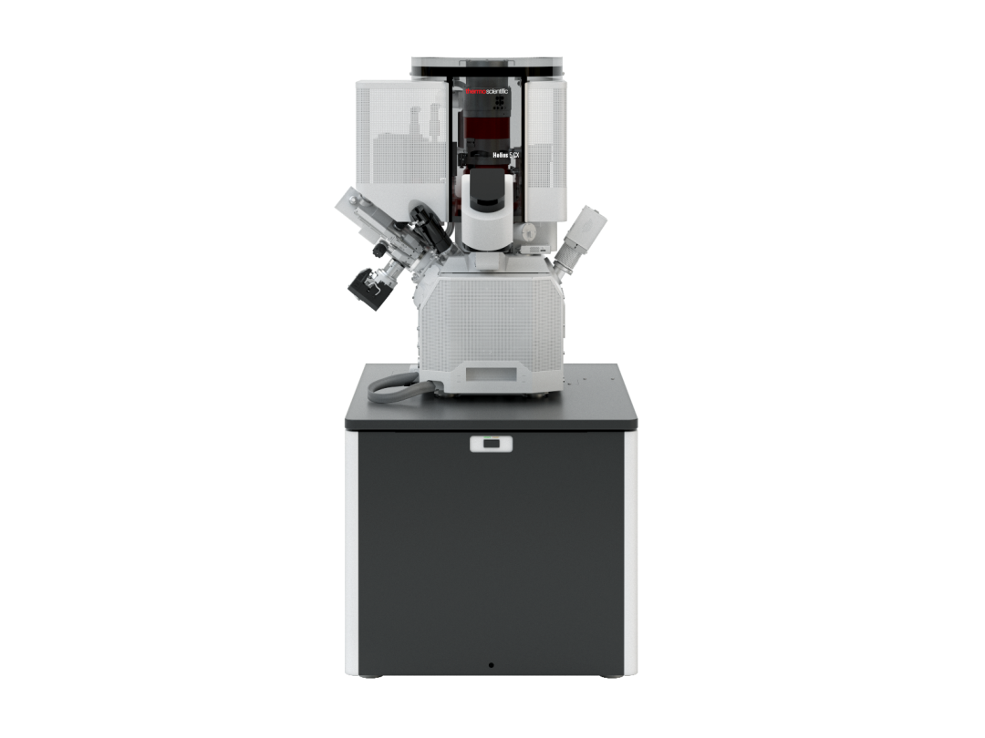
The Helios 5 Ga+ is a field-emission focused ion beam scanning electron microscope (FIB-SEM) that integrates high-resolution imaging, precise nanofabrication, and 3D characterization capabilities. For advanced ceramic materials, it enables high-resolution observation of micro- and nanostructures—such as grain boundaries, pores, secondary phases, and cracks. By combining high-precision cross-sectioning with 3D reconstruction techniques, it provides deep insights into sintered microstructures, interfacial bonding, and failure mechanisms. Furthermore, the Helios 5 CX supports the integration of analytical techniques like EDS and EBSD, enabling the simultaneous characterization of morphology, crystal structure, and elemental distribution. It offers a comprehensive, efficient micro-analysis solution for the material design, process optimization, and quality control of structural, electronic, and functional ceramics, driving ceramic material research to new heights through advanced hardware performance and intelligent workflows.
Apreo ChemiSEM: Integrated EDS Field-Emission Scanning Electron Microscope
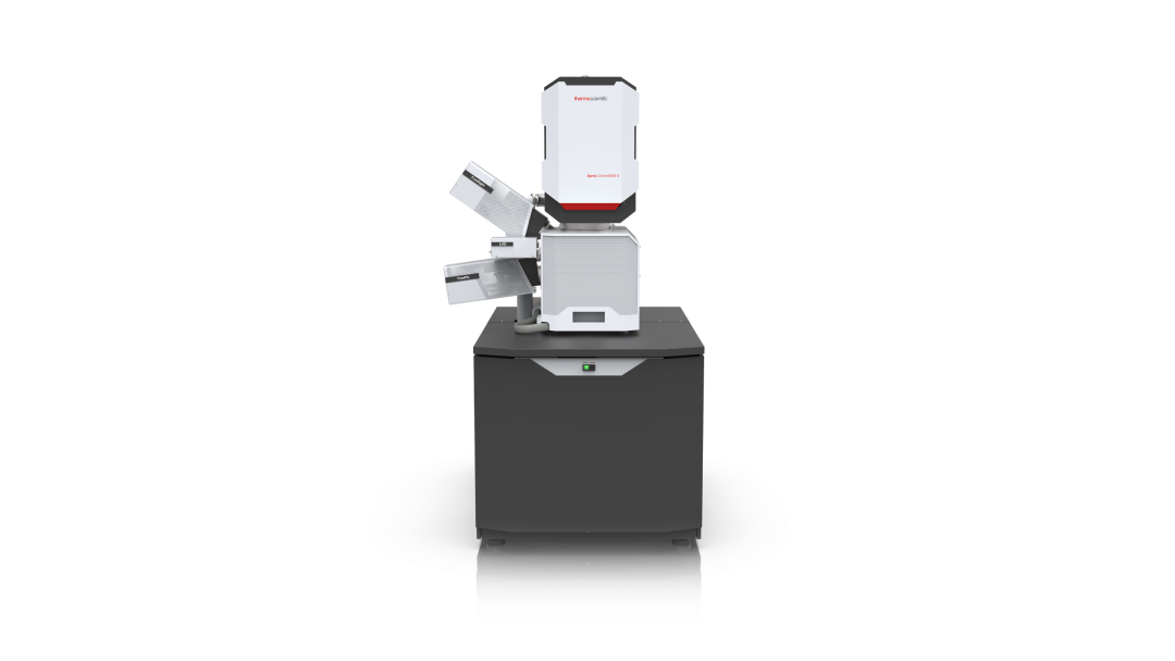
The Thermo Scientific™ Apreo™ ChemiSEM™ scanning electron microscope system integrates the unique Thermo Scientific™ Trinity™ in-column detection system with Thermo Scientific™ ChemiSEM™ technology. By combining high-resolution morphological imaging and elemental analysis capabilities within a single software platform, it delivers a seamless, streamlined workflow that meets the demands of high-throughput, fast-paced laboratories while enabling efficient and reliable analysis of a wide range of samples.
X-ray Photoelectron Spectrometer
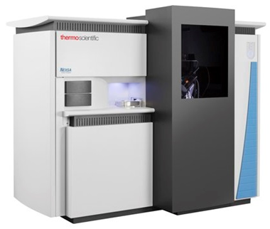
With the advancement of analytical technologies, the study of material surface characteristics and interfacial interactions has become crucial. Thanks to its extreme surface sensitivity, X-ray Photoelectron Spectroscopy (XPS) can analyze and characterize the elemental composition and chemical states of material surfaces within the top 0–10 nm and detect elements ranging from lithium (Li) to uranium (U). It is widely used not only in academic fields—such as chemical analysis, materials research and development, and theoretical physics—but also increasingly in various industrial sectors, including the development of functional nanomaterials, glass coatings, semiconductor devices, and the process evaluation of coating materials.
Recommended Event: [Exhibition Guide] Save the visitor registration link, transportation details, and exhibitor list with one click! Join us at the Shenzhen Precision Ceramics Exhibition from August 26 to 28!
Click the image below 👇 to view conference details and attend for free!
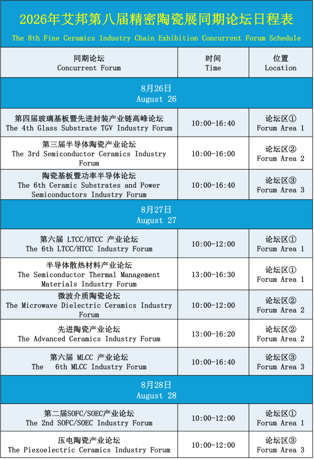
Attendee Pre-registration:
Method 1: Step 1 – Follow the "Aibang Ceramics Exhibition" (艾邦陶瓷展) WeChat official account (scan the QR code below or click the account card); Step 2 – Select "Attendee Registration" from the bottom menu.
Method 2:

Scan the QR code or copy the link to register:
https://www.aibang360.com/sign/100085
2. Professional VIP Attendee Registration:
VIP Attendee Benefits: Complimentary drinking water, lunch voucher, and exhibition directory.
VIP Group Benefits (15+ people): Dedicated shuttle service within Guangdong Province.
Target VIP Audience: Power semiconductor modules (IGBT/SiC/PIM), packaging & testing, MLCC/LTCC/HTCC, electronic ceramic components, ceramic substrates (AMB/DBC/DPC), communication equipment, optical communication modules, 3C consumer electronics, and automotive electronics.
For VIP and group registration, please contact Ms. Wen at 18126443075 (also her WeChat ID).

※ Minors under the age of 18 are not permitted to visit; please do not bring children inside.