
Ningbo Jingzuan: Building a Foundation on CVD Growth and Empowering through Ultra-Precision Machining to Forge Core Diamond Capabilities
Ningbo Jingzuan Technology Co., Ltd. will participate in the 8th Aibang Precision Ceramic Industry Chain Exhibition from August 26 to 28, 2026 (Booth No. H16). We warmly welcome industry colleagues to visit us and exchange ideas!
01 Company Profile
Located in Ningbo, Zhejiang, Ningbo Jingzuan Technology Co., Ltd. operates an R&D center dedicated to CVD diamond production and processing equipment. Leveraging natural and synthetic diamond materials—and utilizing cutting-edge modern manufacturing technologies such as CVD, nanofabrication, and laser-based ultra-precision micro-machining—the company is committed to the R&D, production, sales, and service of diamonds, diamond tools, and related equipment.

The company boasts a team comprising experts from national-level key talent programs, as well as foreign and overseas-educated researchers, professors, and PhDs with cross-industry expertise. It has established a joint technology R&D center with the Ningbo Institute of Materials Technology and Engineering (Chinese Academy of Sciences) and maintains long-term strategic alliances with numerous multinational corporations, universities, and research institutes in Japan and the United States.
Core Business: Large CVD single-crystal diamonds (lab-grown diamonds), ultra-precision single-crystal diamond cutting tools, diamond-based high-thermal-conductivity composite materials and devices, diamond surface nano-modification, diamond abrasive tools (saw blades, grinding wheels, wire saws, etc.), ultra-high vacuum CVD equipment, ultra-precision 3D laser sculpting equipment, and nano-precision diamond tool grinding equipment.
02 Product Introduction
01
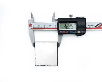
Large-Seed Single-Crystal Diamond
Technical Specifications:
· Large-size (inch-scale) homoepitaxial single-crystal diamond;
· Crystal planes: (100), (110), or (111) available;
· Adjustable boron concentration;
· Surface roughness Ra ≤ 1 nm.
Applications: Widely used in integrated circuit thermal management, ultra-precision machining, optical windows, quantum technology, and more.
02
Ultra-thin Single-crystal Diamond
Technical Specifications:
Thickness: 10–200 μm;
Crystal Plane: (100);
Thermal Conductivity: ≥2300 W/(m·K).
Applications: Widely used in integrated circuit thermal management, ultra-precision machining, optical windows, quantum technology, etc.

03
Gold-Plated Diamond Heat Spreader
Technical Specifications:
· Customizable dimensions;
· Thermal conductivity ≥ 2300 W/(m·K);
· Customizable surface metal patterning;
· Temperature resistance ≥ 350°C.
Applications:
· Heat spreading substrate for high-power solid-state lasers
· Heat spreading substrate for radar power devices

04
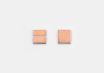
Copper-Plated Diamond Heat Sink
Technical Specifications:
· Customizable dimensions;
· Thermal conductivity ≥ 2300 W/(m·K);
· Customizable surface metal patterning.
Application: Heat dissipation substrate for high-power inverters.
05
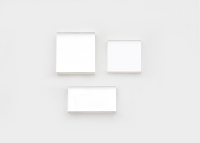
Diamond Optical Windows
Technical Specifications:
· Dimensions: Customized;
· Optical transmission (after coating): ≥71%;
· Surface roughness (Ra): <1 nm;
· TTV: <5 μm.
Applications:
· High-power laser systems
· Infrared optical systems
· X-ray windows
· Synchrotron radiation windows
· Semiconductor manufacturing
· Detectors
· Accelerators
· Hypersonic vehicles/satellites
06
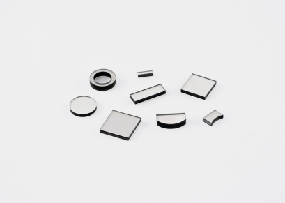
Mechanical-Grade Single-Crystal Diamond
Technical Specifications:
· Crystal planes: (100), (110), or (111) available;
· Hardness: 10 (Mohs scale);
· Thermal conductivity: ≥2000 W/(m·K);
· Coefficient of friction: 0.05–0.10.
Applications:
· Ultra-precision cutting tools (turning, milling, and engraving tools, etc.)
· Medical ophthalmic surgical knives
· Medical tissue sectioning knives
07
Single-Crystal Diamond Wire Drawing Die
Technical Specifications:
· Crystal orientation: (100), (110), or (111) (selectable);
· Customizable dimensions;
· Hole diameter: ≥30 μm;
· Customizable drawing hole shape (round, elliptical, conical, etc.).
Applications:
Wire drawing of metals and alloys such as copper, tungsten, molybdenum, gold, and silver (primarily for fine and ultra-fine wire drawing).
08
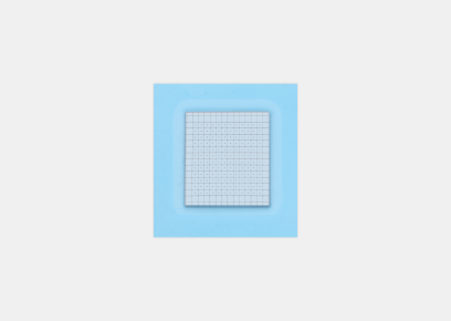
CMP Conditioner
Technical Specifications:
· Free from metal contamination;
· Reconditionable for repeated use;
· No particle shedding;
· Service life is more than five times that of traditional conditioners.
Applications:
· Wafer material manufacturing
· Packaging and testing
· Optical component manufacturing
· Titanium alloy processing
09
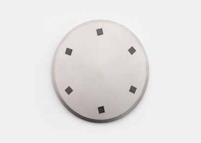
Ultra-high surface quality diamond
Technical specifications: Ra < 0.2 nm

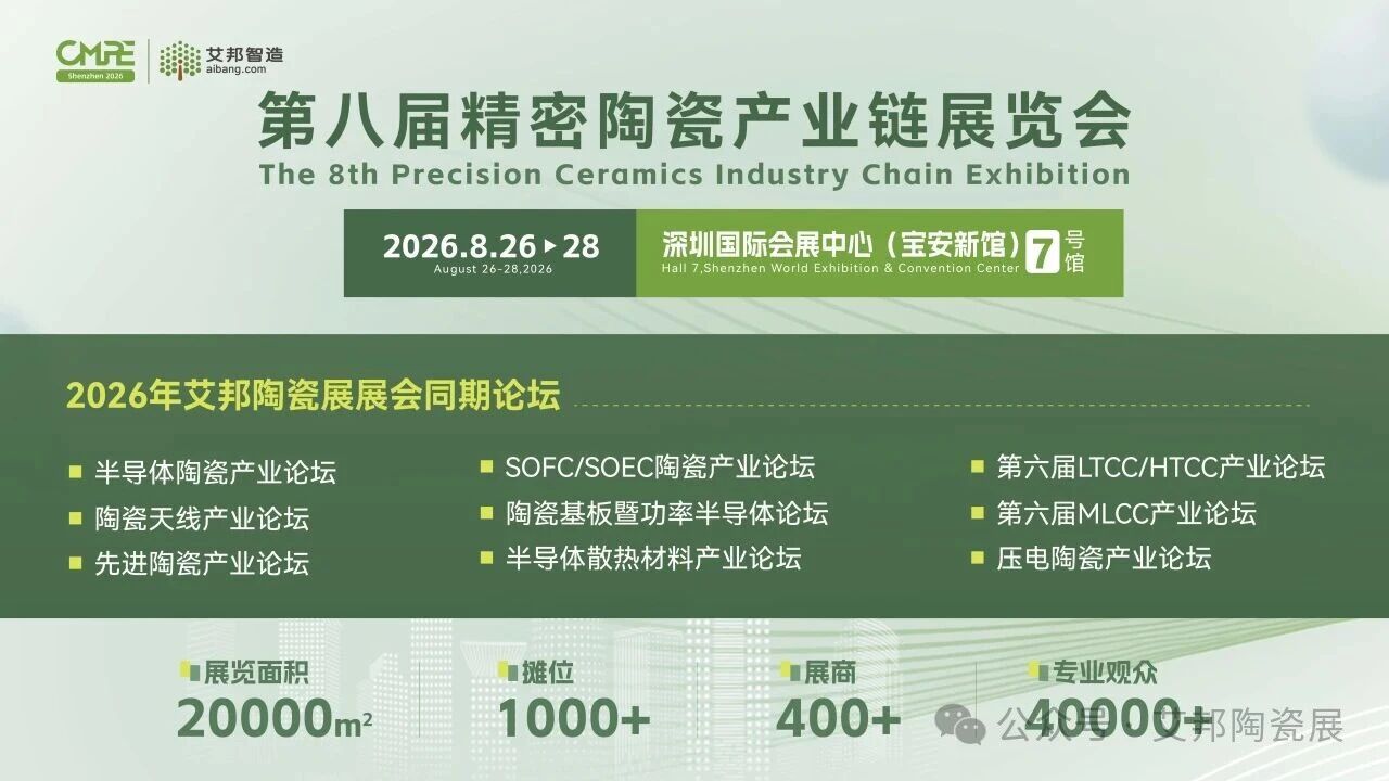
Recommended Event 1: Aibang’s 8th Precision Ceramics Industry Chain Exhibition [August 26–28, 2026 | Hall 7, Shenzhen World Exhibition & Convention Center (Bao'an New Venue)]
Booth Booking
Ms. Li: 18823755657 (WeChat ID)
Email: lirongrong@aibang.com
Scan the QR code to add on WeChat and inquire about exhibition details.

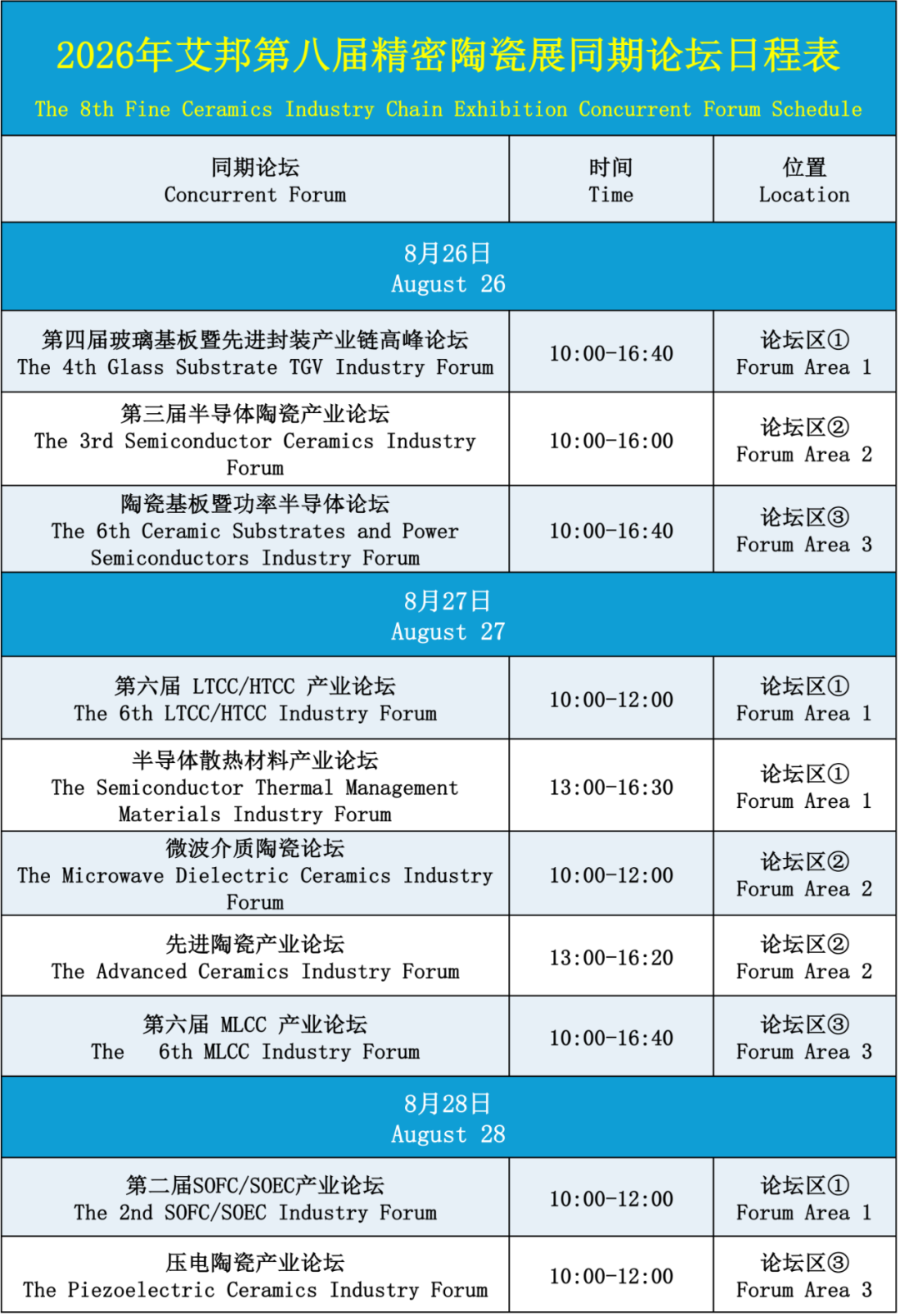
Recommended Event #2: One-Click Registration | Attend 10 Themed Forums for Free at the Shenzhen Precision Ceramics Exhibition (August 26–28)!
[Free Attendance] How to Register:

Scan the QR code or copy the link to register.