
[Free Concurrent Forum] Ceramic Substrate and Power Semiconductor Industry Forum (August 26 · Shenzhen)
Ceramic Substrate and Power Semiconductor Industry Forum
Invitation
August 26, 2026
Hall 7, Bao'an New Hall, Shenzhen World Exhibition & Convention Center
1 Conference Background
As strategic emerging industries—such as new energy vehicles, photovoltaic energy storage, industrial control, and rail transit—enter the stage of large-scale deployment, and as advancements range from the rapid evolution of 5G/6G communications to the upgrading of industrial automation and smart grids, there is a critical reliance on efficient, reliable, and miniaturized power electronics technology. Power semiconductors serve as the core of electrical energy conversion, and their performance directly determines the efficiency and reliability of end products; consequently, the thermal conductivity of ceramic substrates and the reliability of packaging processes are the keys to overcoming bottlenecks regarding high power density, miniaturization, and long service life in power semiconductors.
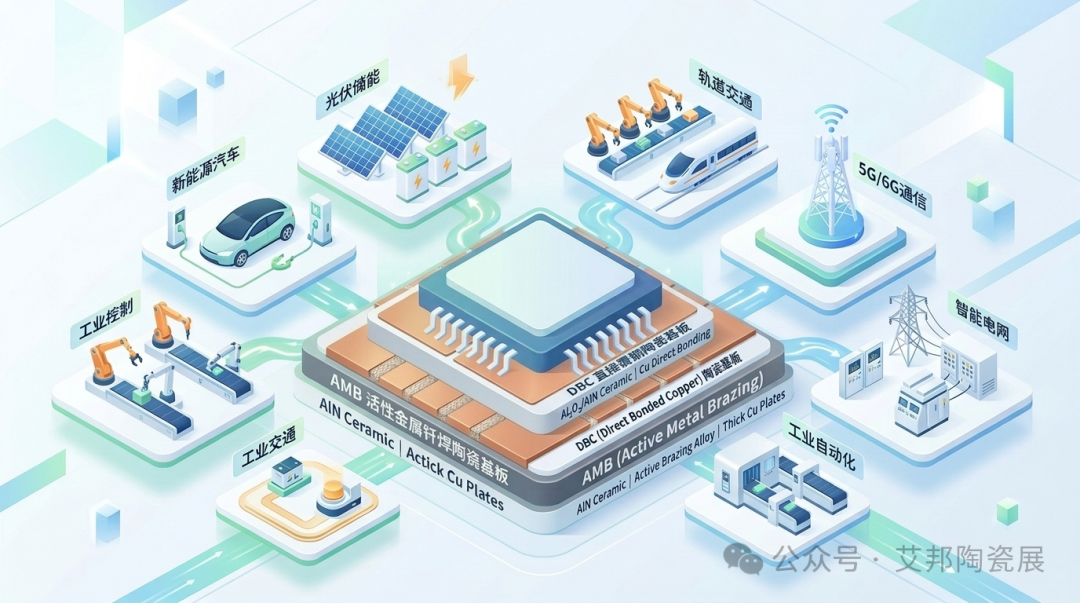
The application of microelectronic devices and third-generation semiconductors is currently trending toward high integration and high performance; however, the resulting surge in power density and heat generation severely limits device reliability and lifespan. Consequently, developing novel packaging materials that combine high thermal conductivity with excellent overall performance has become key to addressing this challenge. Thanks to their outstanding insulation, high thermal conductivity, coefficient of thermal expansion matched to that of the chip, and excellent mechanical strength, ceramic substrates have become indispensable packaging materials for high-power, high-frequency, and high-temperature applications.
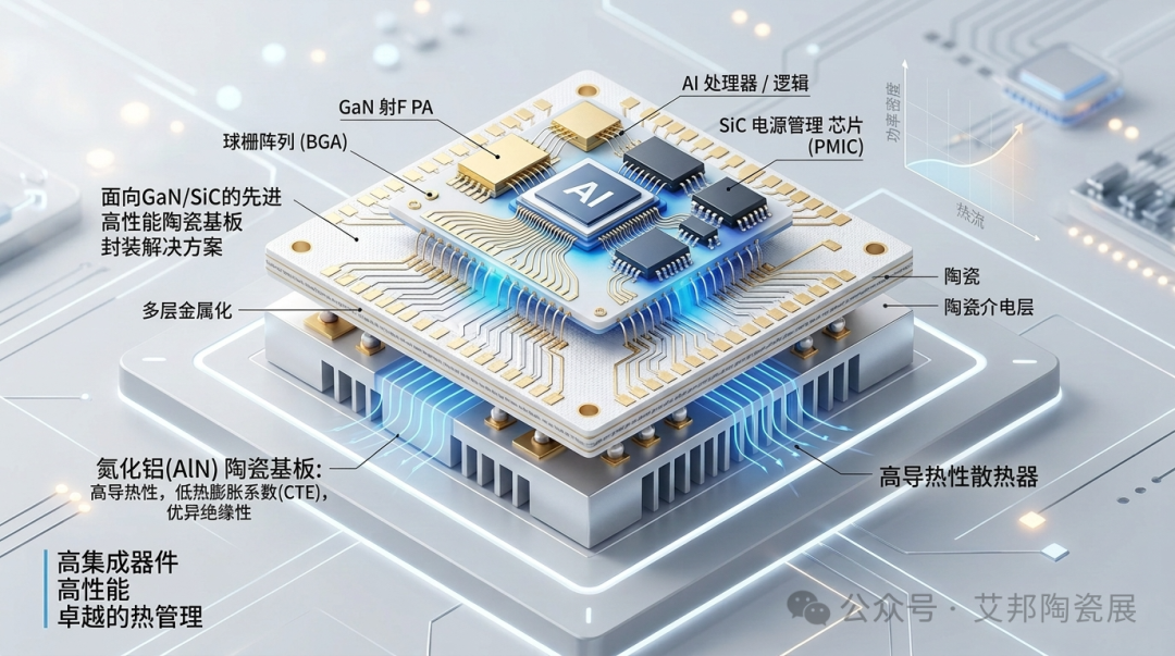
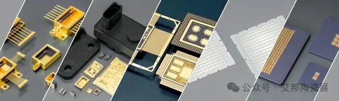
Ceramic material systems primarily include aluminum oxide, aluminum nitride, and silicon nitride. Among them, aluminum nitride has become the preferred choice for high-power LEDs, lasers, and IGBT modules due to its thermal conductivity, which far exceeds that of aluminum oxide. Silicon nitride, combining high thermal conductivity with exceptional mechanical strength, is an ideal material for applications involving severe thermal cycling, such as in electric vehicle inverters. Ceramic packaging is a hermetic technology that protects electronic chips, creating a stable operating environment isolated from external moisture and contaminants; while it offers superior performance compared to lower-cost plastic packaging, it comes at a higher price point. Unlike metal packaging, it possesses inherent electrical insulation advantages. However, the ongoing drive for cost reduction and efficiency improvement, combined with continuous advancements in plastic packaging technology, presents new challenges for ceramic packaging. To withstand these pressures and the competitive impact of plastic packaging, ceramic packaging must leverage its core strengths—high-temperature resistance, high reliability, and excellent heat dissipation—by accelerating technological innovation and precisely targeting high-end electronic application niches to deepen its suitability.
Power semiconductors are central to the field of power electronics; as critical components for energy conversion, they drive improvements in efficiency and stability across sectors such as new energy vehicles, photovoltaic energy storage, and smart home systems. Their functions encompass power conversion, amplification, switching, and circuit protection. IGBTs and MOSFETs are the mainstream products, dominating high-voltage and low-voltage applications respectively. While silicon remains the dominant material, wide-bandgap materials like silicon carbide (SiC) and gallium nitride (GaN) are gradually gaining ground due to their superior properties, though next-generation SiC and GaN devices still face challenges such as material defects.
Currently, power semiconductors are evolving toward higher power density, miniaturization, greater efficiency, and enhanced reliability, making advancements in chip and packaging technologies crucial. Power module packaging requires the integration of chips with components such as ceramic substrates and lead frames to ensure optimal chip performance; however, the surge in power density resulting from dense packaging creates immense pressure regarding voltage drop management and heat dissipation. Furthermore, traditional isolation technologies are approaching their performance limits under high-frequency and high-voltage conditions, thereby constraining overall system efficiency and safety.
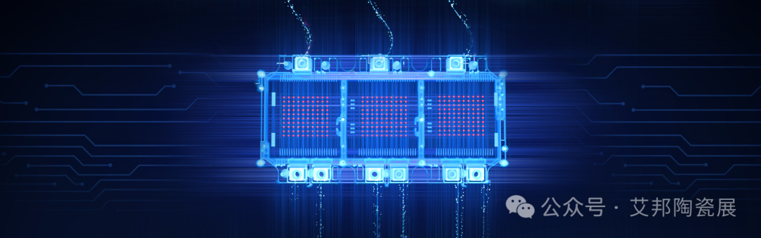
Image source: BYD Semiconductor
The power semiconductor sector encompasses the entire value chain, ranging from the supply of raw materials and equipment—such as wafers, lithography machines, lead frames, wide-bandgap materials, and auxiliary supplies—to R&D, design, manufacturing, packaging, and testing, as well as downstream application markets. Currently, collaboration across the upstream and downstream segments remains insufficient; overcoming these bottlenecks requires a concerted effort involving material innovation, technological advancement, and industry-wide synergy.
Against this backdrop, achieving breakthroughs in power semiconductor performance and ensuring reliable application relies heavily on the efficient thermal conductivity provided by ceramic substrates and the precision protection offered by ceramic packaging. To foster this progress, Aibang Smart Manufacturing will host the "Ceramic Packaging and Power Semiconductor Industry Forum" on August 26, 2026, at Hall 7 of the Shenzhen World Exhibition & Convention Center (Bao'an New Hall). Held concurrently with the Aibang Precision Ceramics Exhibition—an event that gathers key players from across the supply chain—the forum will focus on topics such as ceramic materials, packaging processes, power semiconductor chips, and their applications. We cordially invite industry experts, corporate representatives, and researchers to join us in exploring new pathways for technological integration and discussing emerging opportunities for industry development.
2 Date and Venue
August 26, 2026; Forum Area ②, Aibang 8th Precision Ceramics Exhibition
3 Proposed Topics
(Topics updated as of July 10)
No. | Proposed Topic | Invited Speaker |
1 | Innovation in Embedded Packaging Technology Based on DAB Ceramic Substrates | Liu Heng, Head of Strategic Planning Department, Jiangsu Ferrotec Power Semiconductor Research Institute Co., Ltd. |
2 | Silver-Free AMB Copper-Clad Ceramic Substrates for High-Voltage Power Modules: Material Innovation and Reliability Research | Chen Tianhua, Deputy General Manager, Jiangsu Hansirui Semiconductor Technology Co., Ltd. |
3 | Application of Precision Laser Processing and Welding Technologies in High-Reliability Power Device Packaging | Zhao Jiantao, General Manager, Zhejiang Zichen Laser Intelligent Equipment Co., Ltd. |
4 | Silicon Nitride Powder Project via Ammonolysis | Liu Zaixiang, General Manager, Qingdao Qiaohai Ceramic New Materials Technology Co., Ltd. |
5 | Key Technologies and Innovative Applications of DPC Ceramic Substrates for Advanced Packaging | Wu Zhaohui, General Manager, Jiangxi Jinghong New Material Technology Co., Ltd. |
6 | Pioneering Comprehensive Innovative Applications of High-Reliability Silicon Nitride Copper-Clad Ceramic Substrates in New Energy Vehicles, PV Energy Storage, and Industrial Power Modules | Zhou Xin, General Manager, Nantong Wisper Semiconductor Technology Co., Ltd. |
7 | Securing a Position in Domestic Substitution: Mass Production Value and Application Prospects of 92% Alumina Ceramic Substrates | Pan Zimei, Engineer, Guangdong Ciyuanchuangxin Semiconductor Co., Ltd. |
8 | Application of PVD Technology on Ceramic Substrates for Packaging | Xie Bin, Professor, University of Science and Technology of China (USTC) |
9 | Research Progress on the Structure of IGBT Devices | Professor Zhang Jinping, University of Electronic Science and Technology of China |
10 | Applications and Development of High-Performance Aluminum Nitride Ceramics | Wang Mingqing, Deputy Chief Engineer, Chengdu Xuci / Ningxia Beici |
11 | Application of Magnetron Sputtering for Deep-Hole Coating on Ceramic Substrates | Guangdong Huicheng Vacuum Technology Co., Ltd. |
12 | Industrialization and Application of High-Thermal-Conductivity Ceramic Substrates | Peng Xiang, Deputy General Manager/Chief Engineer, Yibin Hongxing Electronics Co., Ltd. |
13 | Topic to be Determined | Hunan Jinbo Carbon Co., Ltd. |
14 | Discussion on the Application of Silver-Coated Copper in Silver Pastes for Chip Interconnects | Professor Li Minggang, Central South University |
15 | Application of Defect Detection in Precision Ceramic Manufacturing Processes | Liu Weisheng, Deputy General Manager, Shenzhen Hesizhongcheng Technology Co., Ltd. |
We are currently soliciting additional topics; recommendations or self-proposed topics are welcome. For speaking or sponsorship inquiries, please contact Ms. Li at 18124643204 (also her WeChat ID).

Long-press the QR code to register online.

Alternatively, copy the link to your browser to register via WeChat: https://www.aibang360.com/m/100308
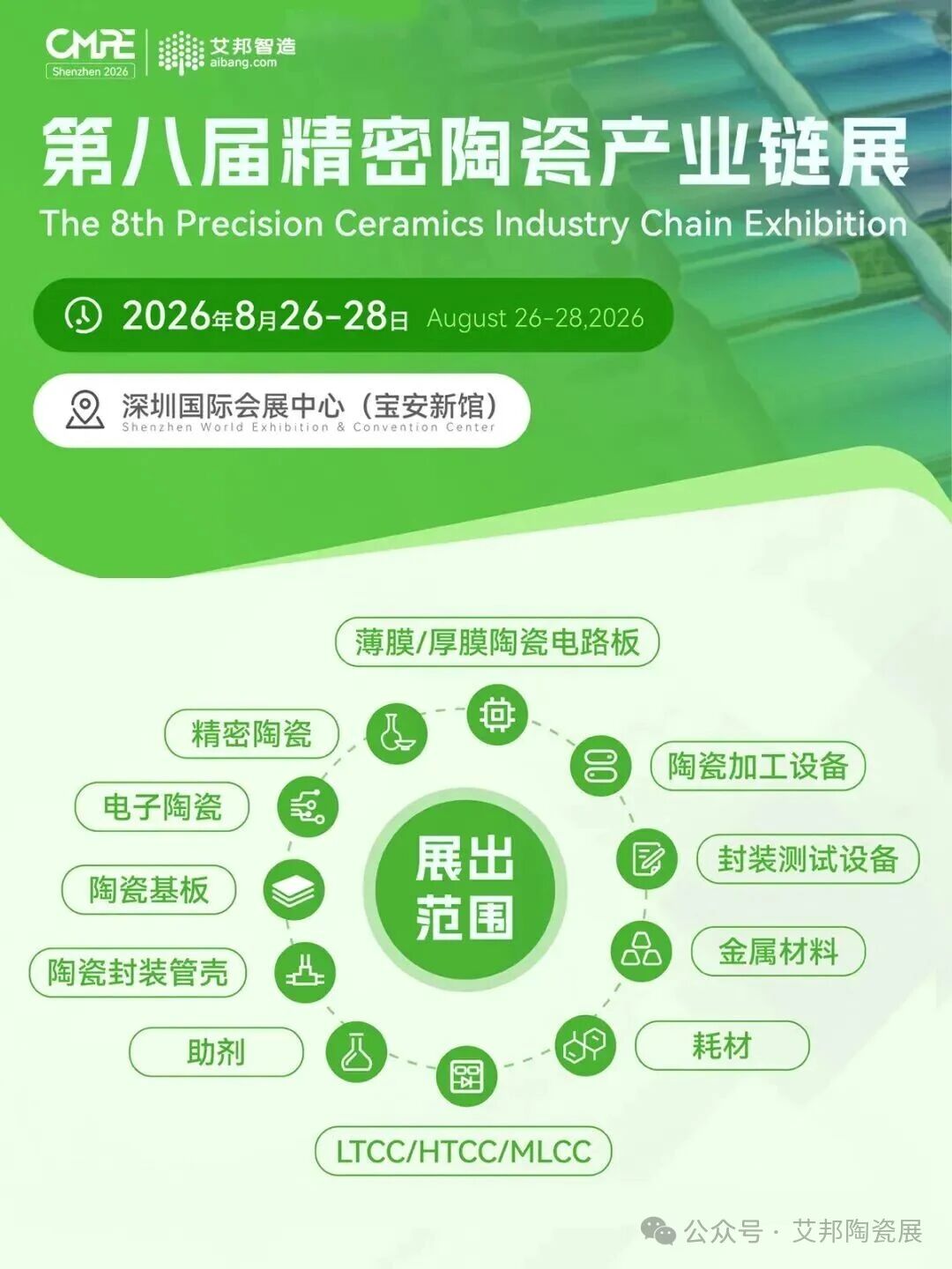
Recommended Event 2: Aibang’s 8th Precision Ceramics Industry Chain Exhibition [August 26–28, 2026 | Shenzhen World Exhibition & Convention Center (Bao'an New Hall)]
Booth Booking
Ms. Wen: 18126443075 (WeChat ID)
Email: wenxiaoting@aibang.com
Scan the QR code to add on WeChat and inquire about exhibition details.