
Technology-Driven, Smart Manufacturing for the Future | Feishida Empowers High-End Semiconductor and PCB Manufacturing Processes
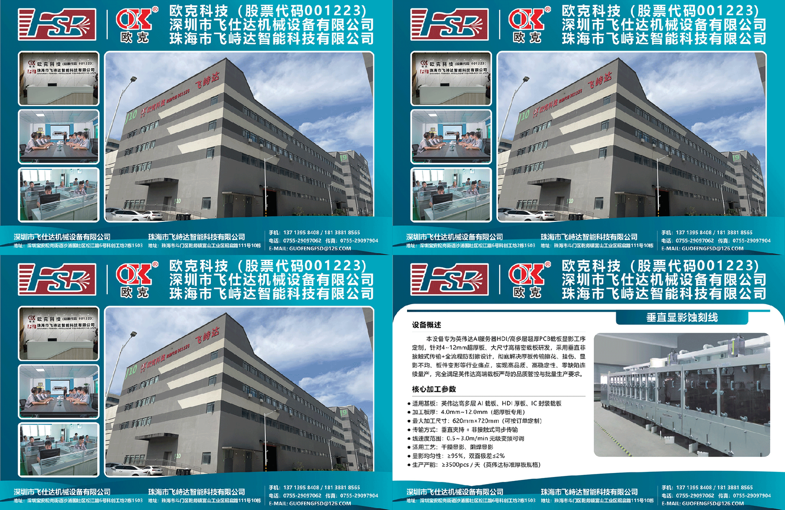

Shenzhen Feishida Machinery Equipment Co., Ltd. was established in 2010. In March 2026, it was acquired by the publicly listed company Ouke Technology (Stock Code: 001223), gaining significant support in both technology and capital. Headquartered in Songgang Subdistrict, Shenzhen, the company established a subsidiary—Zhuhai Feizhida Intelligent Technology Co., Ltd.—in the Fushan Industrial Zone of Doumen District, Zhuhai, in 2024. The company operates a dedicated 30,000-square-meter factory complex and employs over 200 technical staff, including 100 experts with more than a decade of industry experience.
The company specializes in the R&D, production, and sales of equipment for PCBs, FPCs, multilayer boards, HDI boards, precision metal etching, lead frames, and semiconductor ceramic substrates. Its product portfolio encompasses high-end semiconductor equipment—such as DBC, DPC, and AMB lines—and includes specific systems for developing, vacuum etching, titanium/film stripping, anti-oxidation treatment, silver immersion, automatic board grinding (including ceramic substrates), polishing, copper reduction, pre-treatment, brown oxide treatment, sandblasting, and finished product cleaning. Currently, the company serves clients across regions including Shanghai, Chongqing, Jiangxi, Hubei, Hunan, Shandong, Zhejiang, and Sichuan, supporting dozens of high-end ceramic substrate manufacturers. Feishida is confident that, through advanced technology and high-end products, it will reach new heights, achieve greater longevity, and expand its horizons within the semiconductor industry.
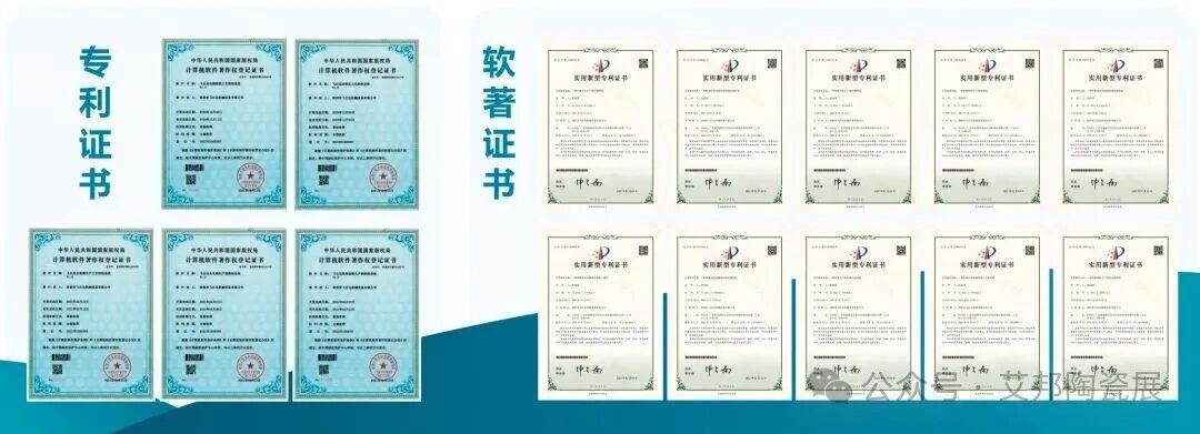
Flagship Product
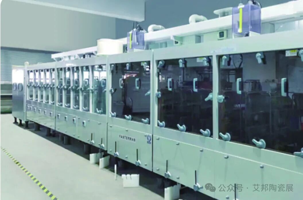
Vertical Developing Machine Technology
Specially Designed for NVIDIA Ultra-Thick Boards
01
Equipment Overview
This equipment is custom-engineered for the developing process of NVIDIA AI server HDI and high-layer-count, ultra-thick PCB substrates. Designed specifically for ultra-thick boards (4–12 mm) and large-format, high-precision substrates, it utilizes a vertical non-contact transport system combined with a scratch-prevention design throughout the entire process. It effectively resolves industry pain points—such as surface scratches, abrasions, uneven development, and board deformation—associated with transporting thick boards. The system enables high-quality, highly stable, and defect-free continuous mass production, fully meeting NVIDIA’s rigorous quality control and volume production standards for high-end substrates.
02
Key Processing Parameters
1. Applicable Substrates: NVIDIA high-layer-count AI substrates, HDI thick boards, IC packaging substrates
2. Processing Thickness: 4.0 mm – 12.0 mm (optimized for ultra-thick boards)
3. Max. Processing Size: 620 mm × 720 mm (customizable upon request)
4. Transport Method: Vertical clamping + non-contact synchronous transport
5. Line Speed Range: 0.5 – 3.0 m/min (continuously adjustable via VFD)
6. Applicable Processes: Dry film developing, solder mask developing
7. Development Uniformity: ≥95%; double-sided variation ≤2%
8. Production Capacity: ≥3,500 pcs/day (based on NVIDIA standard thick board specifications)
03
Core Advantages in Quality Assurance
1. Zero-Defect Guarantee: Employs a fully non-contact and flexible clamping process, completely eliminating defects such as scuffs, scratches, clamp marks, and impact damage; achieves a yield rate of ≥99.8%.
2. Heavy-Duty/Thick Board Compatibility: Features a specialized heavy-load vertical structure that ensures stable transport of ultra-thick boards (4–12 mm) without deformation or jamming.
3. Stable Mass Production: Utilizes fully automated closed-loop control to ensure consistent parameters, enabling stable, uninterrupted 24-hour production.
4. High-End Application Ready: Fully meets the stringent high-precision and high-reliability standards required for NVIDIA AI carrier boards, ensuring successful mass production and delivery of high-end orders.
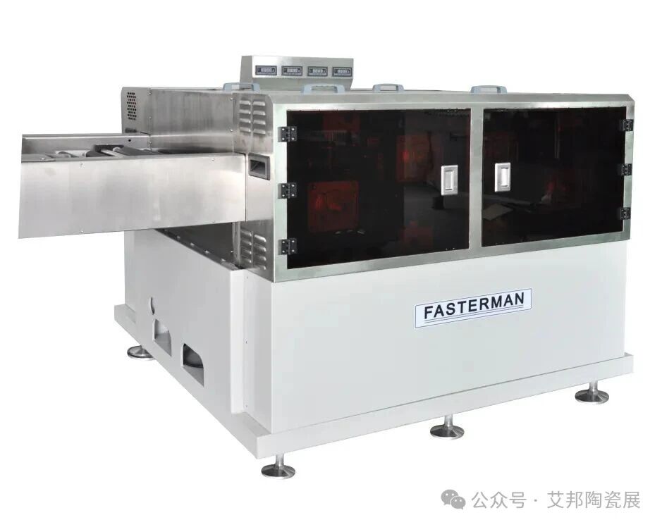
Heavy-Duty Machine for Ultra-Thick Boards with Resin Via Plugging
01
Equipment Overview
This resin-plugging template grinding machine is a precision grinding system designed specifically for the PCB industry. Engineered for the processing of resin-plugging templates—including grinding, copper reduction, and surface finishing—it handles a full range of thicknesses from ultra-thin (0.1 mm) to ultra-thick (12 mm) boards. It balances the need to prevent deformation in ultra-thin boards with the requirement for heavy-duty grinding on thick boards. Featuring high structural rigidity, superior grinding precision, and stable operation, the machine perfectly supports the complete process flow—including rough grinding, fine grinding, and refinishing—meeting the diverse template processing needs of various PCB manufacturers.
02
Basic Processing Parameters
1. Processing board thickness range: 0.3 mm – 12 mm
2. Applicable template types: Specialized PCB resin-plugging templates, metal templates, precision tooling templates
3. Effective worktable processing dimensions: (Customizable upon request) Standard models: 6250 mm × 6250 mm, 730 mm × 730 mm
4. Single-pass grinding depth: 0.01 mm – 0.2 mm (adjustable to 0.3 mm for rough grinding of thick boards)
5. Accommodates a wide range of thicknesses: ultra-thin 0.1mm panels remain flat and scratch-free, while 12mm thick panels undergo grinding without deformation and meet precision standards;
6. Optimized for PCB resin-plugging stencil processes; the ground surface is smooth and burr-free, ensuring plugging precision remains unaffected;
7. Powerful spindle drive ensures high efficiency when grinding thick panels with large stock removal, while maintaining consistent quality during precision grinding of thin panels;
8. Low operating noise and low failure rate; suitable for long-term, continuous mass production;
9. Simple operation and easy setup, allowing for rapid switching between processing stencils of different thicknesses.
Ultra-thick panels with high thickness-to-diameter ratios
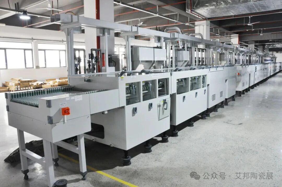
Horizontal electroless copper plating line with integrated desmear capability
01
Equipment Overview
This horizontal electroless copper plating line is specialized equipment for high-end PCB manufacturing. It integrates a fully automated desmear process with horizontal electroless copper plating. Designed specifically for 6mm ultra-thick PCBs and through-holes with high aspect ratios, it achieves flawless metallization for holes with an ultra-high aspect ratio of 1:25. It effectively resolves industry challenges such as incomplete desmear, uneven copper coverage, and voids within the holes of ultra-thick boards. The system offers stable operation, high process precision, and suitability for high-volume continuous production, meeting the rigorous requirements for electroless copper plating on high-layer-count PCBs, thick PCBs, and high-end IC substrates.
02
Key Process Parameters
1. Applicable substrate thickness: 0.1mm – 6.0mm (optimized for ultra-thick boards)
2. Maximum panel size: 720mm × 720mm (customizable)
3. Aspect ratio capability: 1:25 (compatible with ultra-high aspect ratio through-holes)
4. Applicable hole diameter range: 0.15mm – 2.0mm
5. Process flow: Fully automated desmear → Neutralization → Hole conditioning → Micro-etching → Pre-dip → Activation → Acceleration → Horizontal electroless copper plating
6. Line speed: 0.5 – 3.0 m/min (continuously adjustable via variable frequency drive)
7. Electroless copper thickness: 0.3μm – 0.8μm (uniform and controllable)
8. In-hole copper uniformity: ≥92%; no plating skips or voids in high-aspect-ratio holes on ultra-thick boards
Shenzhen Company
Address: Room 1503, Building 2, Kechuang Workshop, No. 6 Songjiang Road, Shapuwei Community, Songgang Subdistrict, Bao'an District, Shenzhen
Zhuhai Company
Address: Building 10, No. 111 Zhaoqi Road, Fushan Industrial Zone, Qianwu Town, Doumen District, Zhuhai
Tel: 0755-29097062
Fax: 0755-29097904
Mobile: 13713958408 / 18138818565
E-mail: guofengfsd@126.com
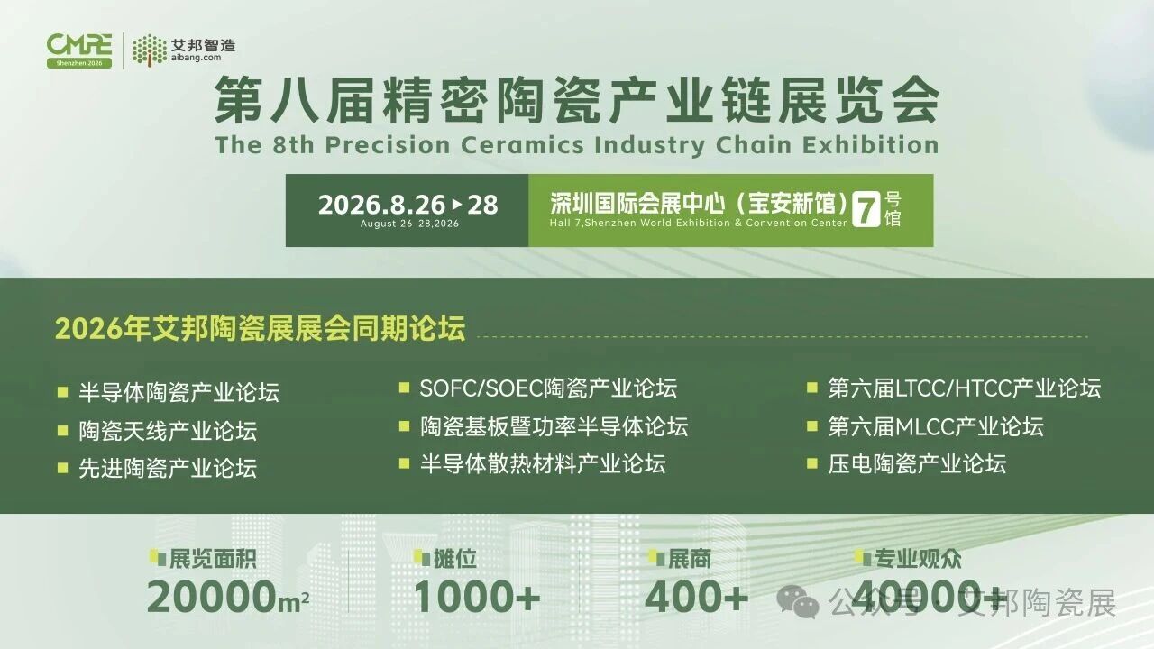
From August 26 to 28, Shenzhen Feishida Machinery Equipment Co., Ltd. will participate in the 8th Aibang Precision Ceramic Industry Chain Exhibition (Booth No. B18). We warmly invite industry colleagues to visit us and exchange ideas!
Recommended Event: The 8th Aibang Precision Ceramic Industry Chain Exhibition [August 26–28, 2026 | Hall 7, Shenzhen World Exhibition & Convention Center (Bao'an New Venue)]
Booth Booking
Ms. Li: 18823755657 (WeChat ID)
Email: lirongrong@aibang.com
Scan the QR code to add on WeChat and inquire about exhibition details.

Recommended Event 2: 9 Concurrent Forums
Concurrent Forums at the 8th Precision Ceramics Industry Chain Exhibition | |
6th LTCC/HTCC Industry Forum | 6th MLCC Industry Forum |
Semiconductor Thermal Management Materials Industry Forum | SOFC/SOEC Industry Forum |
Ceramic Substrate and Power Semiconductor Industry Forum | Advanced Ceramics Industry Forum |
Piezoelectric Ceramics Industry Forum | Semiconductor Ceramics Industry Forum |
Ceramic Antenna Industry Forum | 4th Glass Substrate and Advanced Packaging Industry Chain Summit Forum |
How to register as an attendee:

Scan the QR code or copy the link to register.