
Foda Huakang: A leading enterprise in comprehensive solutions for cavity packaging of domestically produced chips.
Foshan Foda Huakang Technology Co., Ltd. will participate in Aibang’s 8th Precision Ceramics Industry Chain Exhibition from August 26 to 28, 2026 (Booth No. D41). We warmly welcome industry colleagues to visit us and exchange ideas!
Company Profile
Foshan Foda Huakang Technology Co., Ltd. was established in 2005 and is headquartered in Foshan, Guangdong Province. The company was founded by a team comprising outstanding young innovators in science and technology, senior engineers, and experienced professors. It is recognized as a National High-Tech Enterprise, a "Specialized, Refined, Distinctive, and Innovative" (SRDI) enterprise, and a Guangdong Province enterprise integrating industry and education. The company specializes in comprehensive solutions for chip cavity packaging. Its product portfolio includes new materials for chip cavity packaging; B-stage and C-stage epoxy adhesives; B-stage adhesive films and rings; lidded covers made of LCP, ceramic, glass, or metal; ACS, ACC, and QFN cavity packaging housings; and equipment for isothermal cavity packaging and lid-sealing processes. Additionally, the company provides comprehensive technical solutions for the entire isothermal chip cavity packaging process.
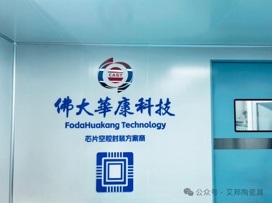
Widely used by R&D and manufacturing enterprises in high-end sectors such as defense electronics, RF communication chips, microwave and radar systems, optical chips, AR/AI chips, optical communication chips, MEMS sensor chips, cavity-packaged chips, power management chips, automotive electronics, and medical devices.
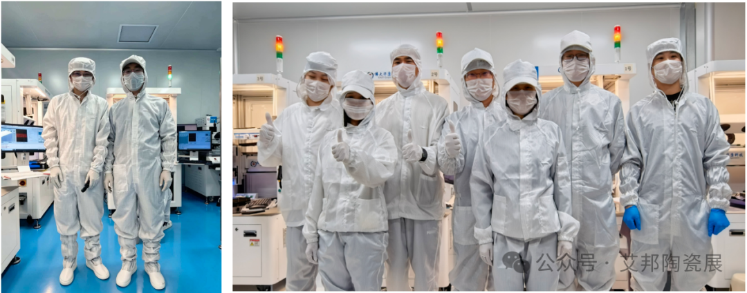
The Aibang Team Visits Foda Huakang
Technological Accumulation
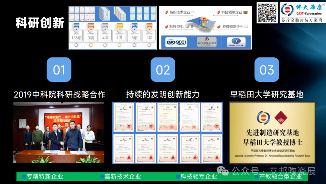
Innovation Achievements: The company has secured a total of 63 patents and computer software copyrights, including 17 granted invention patents and 38 utility model patents. It has received four Guangdong Science and Technology Awards. Its core technologies have overcome critical packaging bottlenecks—such as adhesive overflow and blistering—raising the product yield rate to 99.9%. Leveraging an innovative B-Stage adhesive bonding process, the company provides rapid packaging services for various substrates (including DPC, LTCC, and HTCC), significantly shortening time-to-market. Currently, its products and solutions are widely adopted by leading semiconductor enterprises—such as CETC and Huawei-affiliated companies—spanning high-end sectors including defense electronics, RF, microwave, radar, sensors, optical communications, automotive electronics, and medical devices.
Core Technical Solutions
01
Precision Dispensing Contract Services for B-Stage Adhesive-Coated Lids
■ Process System: A comprehensive, end-to-end solution covering adhesive R&D, dispensing equipment, contract dispensing services, and pre-cured adhesive production;
■ Technical Advantages: Proprietary B-Stage adhesives and vision-guided precision dispensing systems ensure uniform adhesive application and high consistency at the pre-cured interface;
■ Product Portfolio: Pre-glued cover plates (glass, ceramic, PPS, LCP, and metal) and adhesive rings;
■ Product Features: These cover plates come pre-applied with B-Stage adhesive—a process where the adhesive is deposited onto the cover plate along a specific path prior to the chip capping or sealing stage. The pre-applied B-Stage adhesive remains solid at room temperature, facilitating automated handling, storage, and precise alignment during subsequent packaging operations. Upon heating, the adhesive rapidly transitions to the C-Stage (full cure), creating a highly reliable, hermetically sealed structure that significantly boosts yield rates and operational efficiency.
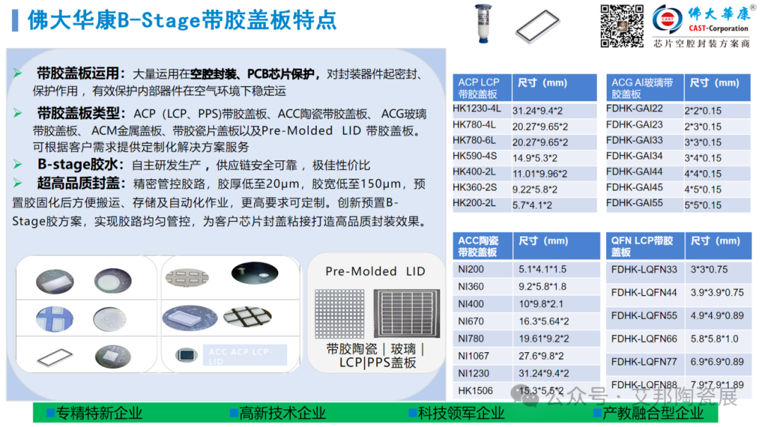
This technology has been successfully applied to 5G RF front-end modules, MEMS sensors, and automotive-grade chip packaging. It moves beyond the traditional multi-step process of dispensing, die-bonding, and curing by integrating adhesive pre-placement with the lid, enabling a controllable three-stage transformation: solid state at room temperature → heat-induced curing → hermetic sealing. Compared to in-situ dispensing, this method eliminates risks such as uneven adhesive distribution, stringing, misalignment, and contamination; it reduces the packaging cycle by over 40% and achieves a stable hermetic sealing yield of 99.98%. The technology is compatible with various substrate and lid material combinations, supporting mainstream lid materials such as LCP, ceramic, glass, and metal.
02
Isothermal Cavity Lid-Sealing System for Chip Packages
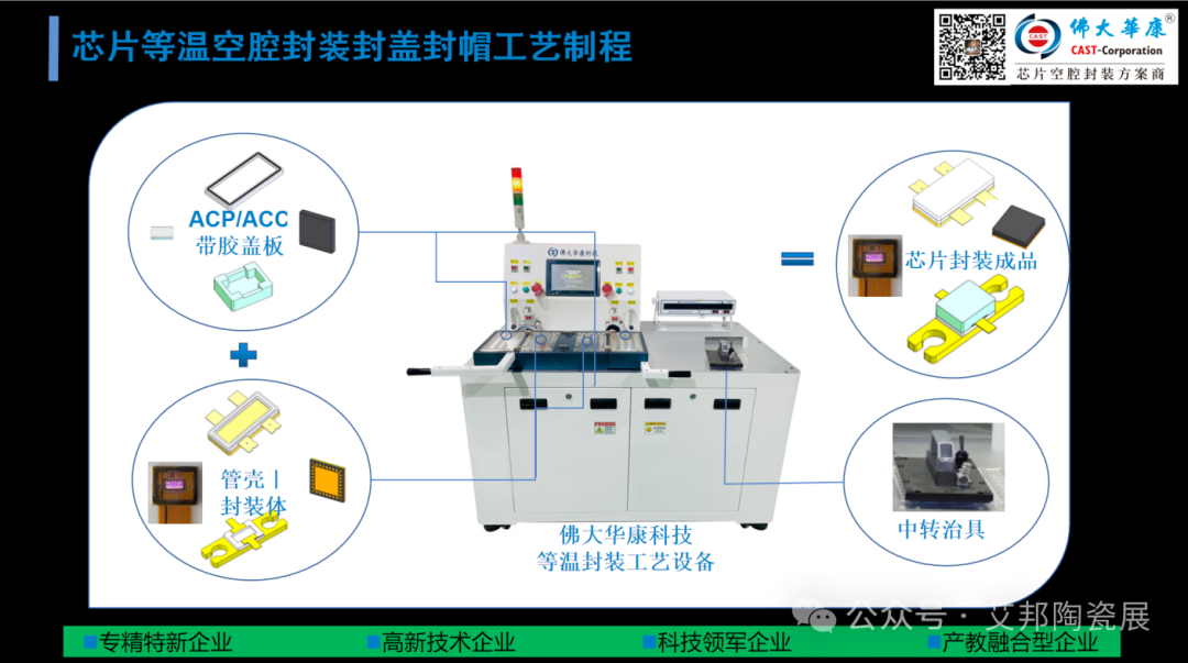
■ Technical Features: Based on proprietary ACP/ACC packaging equipment and patented technologies, the system masters the full process of B-Stage isothermal chip lid-sealing.
■ Patented Process Technology: ● No zonal temperature differences ● No temperature fluctuations ● No temperature overshoot ● Disturbance-free control
Ø Intelligent batch precision packaging Ø AI-driven precision temperature control
Ø Intelligent closed-loop flexible force control Ø Recipe recall and storage functions
Ø Superior, controllable packaging atmosphere Ø Big data technology for historical traceability
Ø ASK-Designer 4.0 intelligent digital software integration
In the B-Stage state, adhesive viscosity increases significantly, effectively limiting adhesive flow. This fundamentally mitigates sealing defects—such as bubbling, perforation, and overflow caused by uncontrolled adhesive movement during the lid-sealing process—thereby ensuring stable and reliable isothermal packaging results.
■ Innovative Breakthroughs: Overcomes ten major technical bottlenecks in the lid-sealing process—including adhesive overflow, adhesive "explosion," bubbling, perforation, leakage, misalignment, and excessive volatile emissions—raising the yield rate to 99.9%.
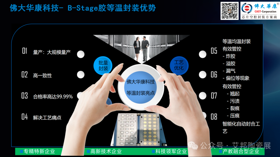
■ Application Value: Facilitates cavity-capping packaging for semiconductor devices—such as pressure sensors, RF chips, and optical chips—that require high reliability. It minimizes performance degradation caused by injection molding contact or localized high temperatures during parallel welding. This solution enables low-cost, high-quality chip capping, helping semiconductor enterprises increase package assembly yields by 20% and reduce time-to-market by 30%.
03
Novel Rapid Package Assembly System
■ Technology Platform: Establishes a modular rapid assembly system by bonding Kovar frames to various substrates (DPC, DBC, AMB, DBA, TPC, TFC, LTCC, HTCC) using a B-stage adhesive process.
■ Engineering Innovation: Leverages proprietary B-stage adhesive technology alongside patented rapid assembly jigs and equipment to develop mass-producible pre-assembled components, reducing the manufacturing cycle for ceramic substrate packages by 60%.
■ Application Scenarios: Particularly suited for specialized packaging requirements (DPC, DBC, AMB, DBA, TPC, TFC, LTCC, HTCC); currently serving high-end sectors including RF devices, power components, sensors, and optical window applications.
04
Innovative B-Stage/C-Stage Epoxy Resin Formulation Technology
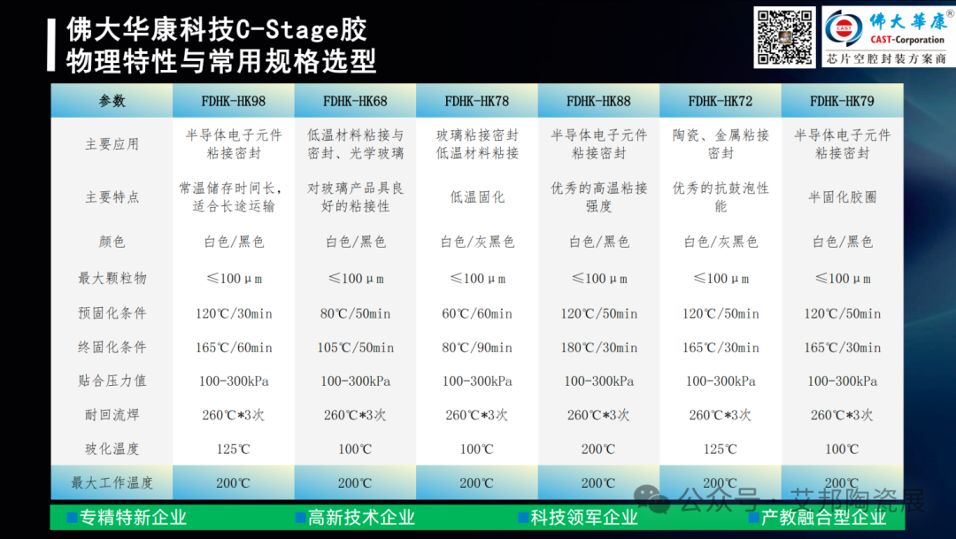
■ Technical Features: 1. B-stage pre-curing capability; 2. Controllable bond-line thickness; 3. Wide curing temperature range; 4. Insulating or conductive options available; 5. High adhesion strength.
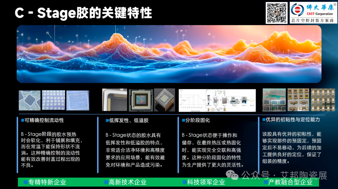
C-Stage Adhesive: 1. Precisely controllable flow: The B-stage adhesive softens upon preheating—facilitating spreading and filling—yet retains its shape without flowing at room temperature. This precise flow control effectively minimizes defects during the capping process. 2. Low volatility and minimal bleed-out: Characterized by low volatility and minimal bleed-out, the B-stage adhesive is ideal for cleanroom environments and high-precision applications, effectively preventing contamination of the environment and the product. 3. Excellent initial tack and precise positioning: The adhesive offers superior initial tack, enabling the pre-fixation of components; once pre-fixed, components remain stable, ensuring accurate positioning for subsequent processing and guaranteeing assembly precision.
■ Customization: Resin systems can be tailored for specific applications (e.g., high-temperature reliability, low dielectric constant, low stress, high thermal conductivity, optical transparency, gold-to-gold bonding, electrical conductivity, insulation, etc.).
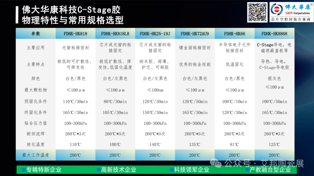
■ Key Performance Indicators:
1. Precisely controlled viscosity-temperature profile (suitable for various processes such as brushing, dispensing, and film molding).
2. Excellent storage stability; high consistency after pre-curing facilitates automated operations.
3. Wide curing window (high process latitude; curing options include 80°C, 100°C, 120°C, 165°C, and 180°C).
4. High bond strength, heat resistance, chemical resistance, low moisture absorption, and superior electrical properties after final cure.
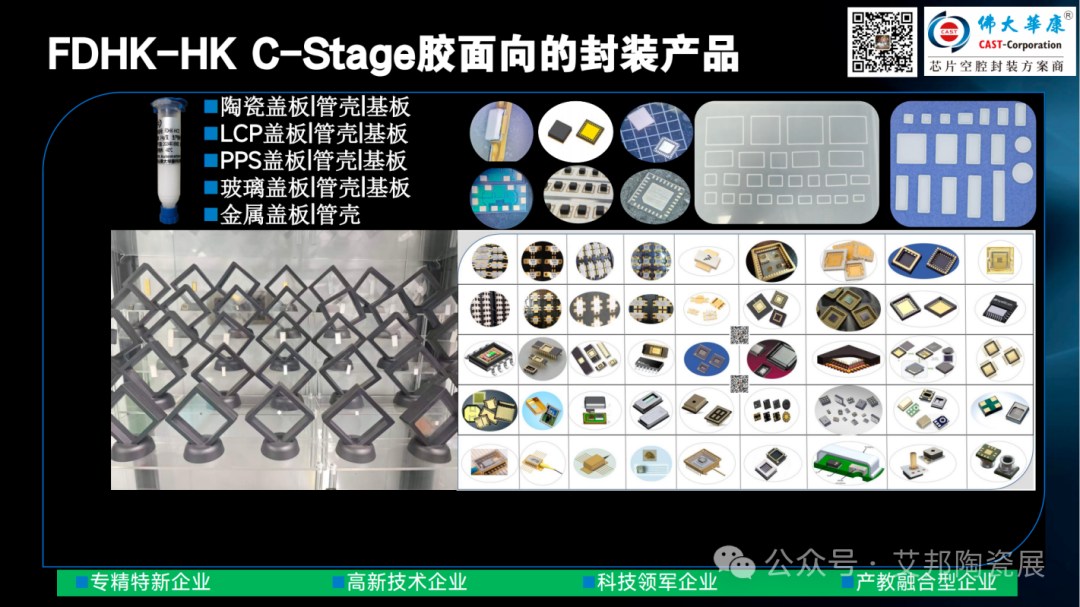
■ Application Areas: Semiconductor packaging | MEMS sensors | Optical lens bonding | Optical module assembly | LCP package lid sealing | Ceramic package sealing
05
Application Examples
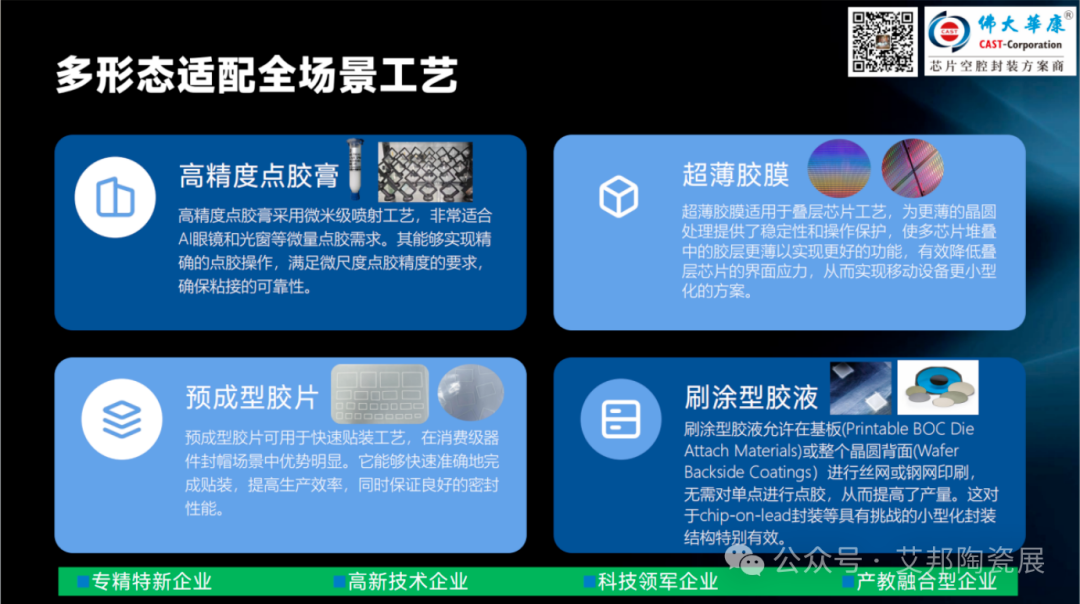
1. High-precision dispensing: Utilizing micron-level jetting technology, this high-precision adhesive is ideal for micro-dispensing applications such as AI glasses and optical windows. It enables precise dispensing operations, meets micro-scale accuracy requirements, and ensures reliable bonding.
2. Ultra-thin adhesive film: Suitable for stacked-chip processes, this film provides stability and handling protection for thinner wafer processing. It allows for thinner adhesive layers in multi-chip stacks—enhancing functionality and effectively reducing interfacial stress—thereby enabling more compact mobile device designs.
3. Pre-formed adhesive film: Designed for rapid placement processes, this material offers distinct advantages in consumer device lid-sealing applications. It enables quick and accurate placement, boosting production efficiency while ensuring excellent sealing performance.
4. Brushable/printable adhesive: Compatible with screen or stencil printing on substrates (Printable BOC Die Attach Materials) or across the entire wafer backside (Wafer Backside Coatings), this material eliminates the need for point-by-point dispensing, thereby increasing throughput. It is particularly effective for challenging miniaturized packaging structures, such as chip-on-lead packages.
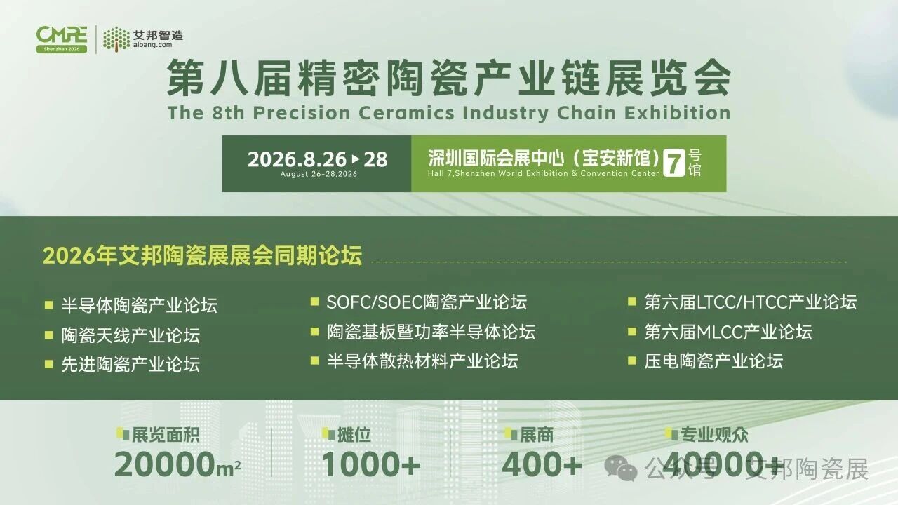
Recommended Event 1: Aibang’s 8th Precision Ceramics Industry Chain Exhibition [August 26–28, 2026 | Hall 7, Shenzhen World Exhibition & Convention Center (Bao'an New Venue)]
Booth Booking
Ms. Li: 18823755657 (WeChat ID)
Email: lirongrong@aibang.com
Scan the QR code to add on WeChat and inquire about exhibition details.

Recommended Event 2: 9 Concurrent Forums
Concurrent Forums at the 8th Precision Ceramics Industry Chain Exhibition | |
6th LTCC/HTCC Industry Forum | 6th MLCC Industry Forum |
Semiconductor Thermal Management Materials Industry Forum | SOFC/SOEC Industry Forum |
Ceramic Substrate and Power Semiconductor Industry Forum | Advanced Ceramics Industry Forum |
Piezoelectric Ceramics Industry Forum | Semiconductor Ceramics Industry Forum |
Ceramic Antenna Industry Forum | 4th Glass Substrate and Advanced Packaging Industry Chain Summit Forum |
How to register as an attendee:

Scan the QR code or copy the link to register.